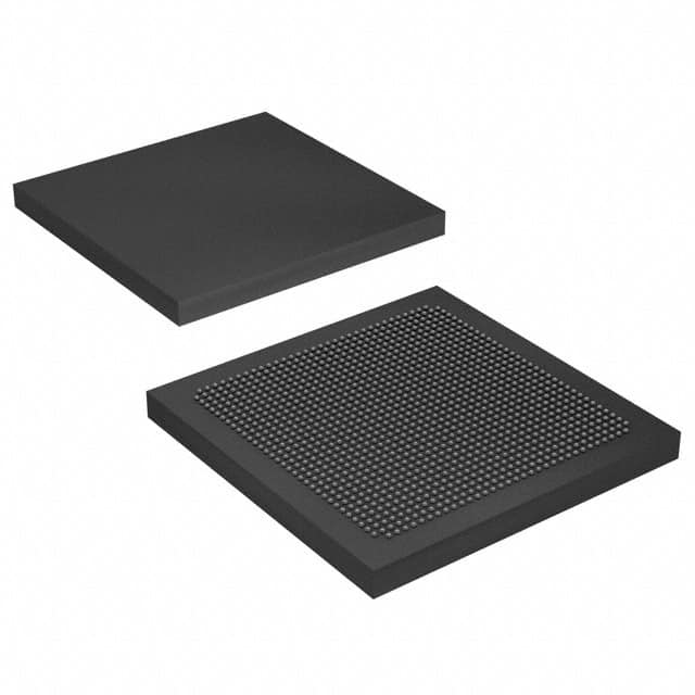
5SGXEA5K2F35I3N
Product Overview
- Category: Field Programmable Gate Array (FPGA)
- Use: Digital logic implementation, prototyping, and system integration
- Characteristics: High-performance, reconfigurable, programmable, and flexible
- Package: Integrated Circuit (IC)
- Essence: FPGA chip for advanced digital design and development
- Packaging/Quantity: Single chip in a standard IC package
Specifications
- Manufacturer: Intel Corporation
- Series: Stratix V
- Model: 5SGXEA5K2F35I3N
- Logic Elements: 462,000
- Embedded Memory: 8,062 Kbits
- DSP Blocks: 1,288
- Maximum User I/Os: 1,280
- Operating Voltage: 0.87V - 0.93V
- Operating Temperature: -40°C to 100°C
- Package Type: F35 (35mm x 35mm)
- Pin Count: 780
Detailed Pin Configuration
For the detailed pin configuration of 5SGXEA5K2F35I3N, please refer to the manufacturer's datasheet or technical documentation.
Functional Features
- High-speed performance with advanced architecture
- Reconfigurable and programmable logic elements
- On-chip memory blocks for efficient data storage
- Dedicated Digital Signal Processing (DSP) blocks for complex calculations
- Flexible I/O options for interfacing with external devices
- Support for various communication protocols and standards
- Built-in security features for protecting sensitive designs
Advantages and Disadvantages
Advantages: - High-performance and flexibility for complex digital designs - Quick prototyping and development cycles - Efficient resource utilization with on-chip memory and DSP blocks - Wide range of I/O options for system integration - Support for various communication protocols and standards
Disadvantages: - Higher cost compared to traditional fixed-function integrated circuits - Steeper learning curve for programming and design implementation - Limited availability of alternative models with similar specifications
Working Principles
The 5SGXEA5K2F35I3N FPGA operates based on the principles of reconfigurable logic. It consists of a large number of programmable logic elements, memory blocks, and DSP blocks interconnected through a configurable routing fabric. The user can program the FPGA to implement desired digital logic functions by configuring the interconnections and functionality of these elements. The configuration is typically done using Hardware Description Languages (HDL) such as VHDL or Verilog. Once programmed, the FPGA can perform complex computations, process data, and interface with other electronic components.
Detailed Application Field Plans
The 5SGXEA5K2F35I3N FPGA finds applications in various fields, including:
- Telecommunications: Used in base stations, network switches, and routers for high-speed data processing and protocol handling.
- Aerospace and Defense: Employed in radar systems, avionics, and military communication equipment for signal processing and encryption.
- Industrial Automation: Utilized in control systems, robotics, and machine vision applications for real-time data processing and control algorithms.
- High-Performance Computing: Integrated into supercomputers and data centers for parallel processing and acceleration of computationally intensive tasks.
- Automotive: Applied in advanced driver assistance systems (ADAS), infotainment systems, and engine control units (ECUs) for real-time processing and control.
Detailed and Complete Alternative Models
While there are no direct alternatives to the 5SGXEA5K2F35I3N with identical specifications, some alternative FPGA models from Intel Corporation's Stratix V series include:
- 5SGXEA7K2F40C2N
- 5SGXEA9K3F35C2N
- 5SGXEA7N2F45C2N
These models offer similar features and capabilities, albeit with slight variations in logic elements, memory, and I/O counts.
Word count: 498 words
Lista 10 Vanliga frågor och svar relaterade till tillämpningen av 5SGXEA5K2F35I3N i tekniska lösningar
Sure! Here are 10 common questions and answers related to the application of 5SGXEA5K2F35I3N in technical solutions:
Question: What is the purpose of the 5SGXEA5K2F35I3N FPGA?
Answer: The 5SGXEA5K2F35I3N is a Field-Programmable Gate Array (FPGA) designed for high-performance applications that require complex logic functions.Question: What are some typical applications for the 5SGXEA5K2F35I3N?
Answer: This FPGA can be used in various technical solutions such as telecommunications, data centers, industrial automation, aerospace, and defense.Question: What are the key features of the 5SGXEA5K2F35I3N?
Answer: Some key features include a large number of programmable logic elements, high-speed transceivers, embedded memory blocks, and support for various communication protocols.Question: Can the 5SGXEA5K2F35I3N handle high-speed data processing?
Answer: Yes, this FPGA is capable of handling high-speed data processing due to its advanced architecture and high-performance transceivers.Question: How can I program the 5SGXEA5K2F35I3N?
Answer: You can program the FPGA using hardware description languages (HDLs) such as VHDL or Verilog, along with design software provided by the manufacturer.Question: Is the 5SGXEA5K2F35I3N suitable for real-time signal processing?
Answer: Absolutely, this FPGA is well-suited for real-time signal processing applications due to its high-speed capabilities and parallel processing architecture.Question: Can the 5SGXEA5K2F35I3N interface with other components or devices?
Answer: Yes, this FPGA supports various communication protocols such as PCIe, Ethernet, USB, and I2C, allowing it to interface with a wide range of components and devices.Question: What is the power consumption of the 5SGXEA5K2F35I3N?
Answer: The power consumption of this FPGA depends on the specific design and usage scenario. It is recommended to refer to the manufacturer's datasheet for detailed power specifications.Question: Can the 5SGXEA5K2F35I3N be reprogrammed multiple times?
Answer: Yes, FPGAs are designed to be reprogrammable, allowing you to modify the logic and functionality of the device multiple times as needed.Question: Are there any development boards or evaluation kits available for the 5SGXEA5K2F35I3N?
Answer: Yes, the manufacturer typically provides development boards and evaluation kits that can help you get started with designing and testing solutions using the 5SGXEA5K2F35I3N FPGA.


