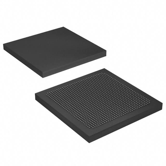
5SGXEA5K2F35I3LN
Product Overview
- Category: Field Programmable Gate Array (FPGA)
- Use: Digital logic circuits, signal processing, and system integration
- Characteristics: High-performance, reconfigurable, programmable, and flexible
- Package: BGA (Ball Grid Array)
- Essence: Advanced integrated circuit for customizable digital designs
- Packaging/Quantity: Single unit per package
Specifications
- Model: 5SGXEA5K2F35I3LN
- Manufacturer: Intel Corporation
- Technology: 28nm
- Logic Elements: 462,000
- Embedded Memory: 8,062 Kbits
- DSP Blocks: 1,288
- Maximum User I/Os: 622
- Operating Voltage: 0.87V - 0.98V
- Operating Temperature: -40°C to 100°C
- Package Dimensions: 35mm x 35mm
Detailed Pin Configuration
The 5SGXEA5K2F35I3LN FPGA has a complex pin configuration with multiple pins dedicated to various functions. For a detailed pin configuration diagram, please refer to the manufacturer's datasheet.
Functional Features
- High-speed performance: The FPGA offers fast processing capabilities, making it suitable for applications requiring real-time data processing.
- Reconfigurability: The device can be programmed and reprogrammed to implement different logic functions, allowing flexibility in design.
- System integration: With its ability to integrate multiple functions into a single chip, the FPGA simplifies system design and reduces component count.
- Low power consumption: The FPGA is designed to operate efficiently, minimizing power consumption while delivering high performance.
- Versatility: It supports a wide range of applications, including digital signal processing, image and video processing, communication systems, and more.
Advantages and Disadvantages
Advantages: - Flexibility in design due to reprogrammability - High-performance processing capabilities - Integration of multiple functions into a single chip - Versatility for various applications
Disadvantages: - Complexity in pin configuration and programming - Higher cost compared to fixed-function integrated circuits - Steeper learning curve for inexperienced users
Working Principles
The 5SGXEA5K2F35I3LN FPGA operates based on the principles of configurable logic blocks (CLBs) and programmable interconnects. The CLBs consist of look-up tables (LUTs), flip-flops, and other components that can be configured to implement desired logic functions. The programmable interconnects allow the routing of signals between different CLBs, enabling the creation of complex digital circuits.
Detailed Application Field Plans
The 5SGXEA5K2F35I3LN FPGA finds applications in various fields, including:
- Telecommunications: Used in base stations, routers, and network switches for signal processing and protocol handling.
- Aerospace and Defense: Employed in radar systems, avionics, and military communication equipment for high-speed data processing and encryption.
- Industrial Automation: Utilized in control systems, robotics, and machine vision applications for real-time data processing and system integration.
- Medical Devices: Integrated into medical imaging systems, patient monitoring devices, and diagnostic equipment for image processing and data analysis.
- Automotive: Applied in advanced driver-assistance systems (ADAS), infotainment systems, and engine control units (ECUs) for sensor fusion and real-time processing.
Detailed and Complete Alternative Models
- 5SGXEA7N2F45C2LN: A higher-end model with increased logic elements and DSP blocks.
- 5SGXEB6R2F40C2N: A lower-cost model with reduced logic elements but similar functionality.
- 5SGXEA9H2F35C2LN: An alternative with higher embedded memory capacity for applications requiring extensive data storage.
These alternative models offer varying specifications and features to cater to different project requirements and budgets.
Word count: 496 words
Lista 10 Vanliga frågor och svar relaterade till tillämpningen av 5SGXEA5K2F35I3LN i tekniska lösningar
Sure! Here are 10 common questions and answers related to the application of 5SGXEA5K2F35I3LN in technical solutions:
Question: What is the 5SGXEA5K2F35I3LN FPGA used for?
Answer: The 5SGXEA5K2F35I3LN FPGA is a Field-Programmable Gate Array that can be used for various applications such as high-performance computing, networking, and signal processing.Question: What are the key features of the 5SGXEA5K2F35I3LN FPGA?
Answer: Some key features of this FPGA include a large number of logic elements, high-speed transceivers, embedded memory blocks, and support for various communication protocols.Question: Can the 5SGXEA5K2F35I3LN FPGA be used for real-time video processing?
Answer: Yes, the high-performance capabilities of this FPGA make it suitable for real-time video processing applications like video encoding, decoding, and image recognition.Question: Is the 5SGXEA5K2F35I3LN FPGA compatible with industry-standard development tools?
Answer: Yes, this FPGA is compatible with popular development tools like Quartus Prime from Intel, which allows users to design, simulate, and program the FPGA.Question: Can the 5SGXEA5K2F35I3LN FPGA be used in safety-critical applications?
Answer: Yes, this FPGA supports functional safety features like error detection and correction, making it suitable for safety-critical applications in industries like automotive and aerospace.Question: What is the power consumption of the 5SGXEA5K2F35I3LN FPGA?
Answer: The power consumption of this FPGA depends on the specific design and usage scenario. It is recommended to refer to the datasheet for detailed power consumption information.Question: Can the 5SGXEA5K2F35I3LN FPGA be used in high-speed networking applications?
Answer: Yes, this FPGA has high-speed transceivers that support protocols like Ethernet, PCIe, and USB, making it suitable for high-speed networking applications.Question: Does the 5SGXEA5K2F35I3LN FPGA support partial reconfiguration?
Answer: Yes, this FPGA supports partial reconfiguration, allowing users to dynamically update specific portions of the design without affecting the entire system.Question: What is the maximum operating frequency of the 5SGXEA5K2F35I3LN FPGA?
Answer: The maximum operating frequency of this FPGA depends on the specific design and implementation. It is recommended to refer to the datasheet for detailed frequency information.Question: Are there any reference designs available for the 5SGXEA5K2F35I3LN FPGA?
Answer: Yes, Intel provides a range of reference designs and application notes that can help users get started with implementing their solutions using the 5SGXEA5K2F35I3LN FPGA.
Please note that the answers provided here are general and may vary depending on the specific requirements and use cases.


