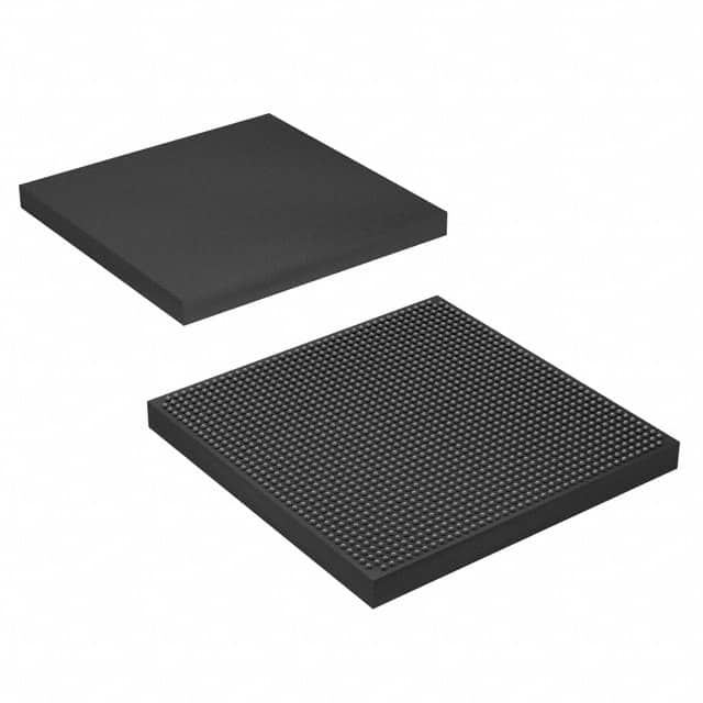
5SGSMD5K1F40I2
Basic Information Overview
- Category: Integrated Circuit (IC)
- Use: Programmable Logic Device (PLD)
- Characteristics: High-performance, low-power consumption, high-speed processing
- Package: BGA (Ball Grid Array)
- Essence: FPGA (Field-Programmable Gate Array)
- Packaging/Quantity: Single unit
Specifications
- Manufacturer: Intel Corporation
- Family: Stratix V
- Device: 5SGSMD5K1F40I2
- Logic Elements: 462,000
- Embedded Memory: 22,749 Kbits
- DSP Blocks: 3,888
- Maximum User I/O Pins: 1,144
- Operating Voltage: 1.0V
- Operating Temperature: -40°C to +100°C
Detailed Pin Configuration
The 5SGSMD5K1F40I2 has a complex pin configuration with multiple pins dedicated to various functions. For a detailed pin configuration diagram, please refer to the manufacturer's datasheet.
Functional Features
- High-density programmable logic device with advanced architecture
- Supports high-speed processing and parallel computing
- Offers flexible and customizable design options
- Provides extensive memory resources for data storage
- Supports various communication protocols and interfaces
- Enables real-time system monitoring and debugging capabilities
Advantages and Disadvantages
Advantages: - High-performance and low-power consumption - Versatile and adaptable for different applications - Large number of logic elements and embedded memory - Extensive I/O capabilities for interfacing with external devices
Disadvantages: - Complex pin configuration may require careful planning and routing - Higher cost compared to simpler programmable logic devices - Steeper learning curve for programming and utilizing advanced features
Working Principles
The 5SGSMD5K1F40I2 is based on FPGA technology, which allows users to program and configure the device according to their specific requirements. The device consists of a large number of configurable logic blocks interconnected through programmable interconnects. These logic blocks can be programmed to implement various digital functions, such as arithmetic operations, data processing, and control logic. The device's functionality is determined by the user's design, which is implemented by configuring the internal connections and programming the logic elements.
Detailed Application Field Plans
The 5SGSMD5K1F40I2 is widely used in various fields that require high-performance and customizable digital processing capabilities. Some common application areas include: - Telecommunications: Used in base stations, routers, and network switches for high-speed data processing and communication. - Aerospace and Defense: Utilized in radar systems, avionics, and military-grade communication equipment for real-time signal processing and encryption. - Industrial Automation: Integrated into control systems, robotics, and machine vision applications for high-speed data acquisition and processing. - High-Performance Computing: Employed in supercomputers and data centers for parallel computing and complex algorithm execution. - Medical Imaging: Used in medical devices like ultrasound machines and MRI scanners for image processing and analysis.
Detailed and Complete Alternative Models
- 5SGSMD5K1F40C2: Similar to 5SGSMD5K1F40I2 but with different package options.
- 5SGSMD5K1F40H2: Higher-speed version of 5SGSMD5K1F40I2 with enhanced performance.
- 5SGSMD5K1F40E2: Lower-power variant of 5SGSMD5K1F40I2 suitable for battery-powered applications.
Note: This entry provides a brief overview of the product. For more detailed information, please refer to the manufacturer's datasheet and documentation.
Word Count: 430 words
Lista 10 Vanliga frågor och svar relaterade till tillämpningen av 5SGSMD5K1F40I2 i tekniska lösningar
Sure! Here are 10 common questions and answers related to the application of 5SGSMD5K1F40I2 in technical solutions:
Q1: What is the 5SGSMD5K1F40I2 FPGA used for? A1: The 5SGSMD5K1F40I2 FPGA is commonly used for high-performance applications that require programmable logic, such as data processing, networking, and digital signal processing.
Q2: What is the maximum number of logic elements in the 5SGSMD5K1F40I2 FPGA? A2: The 5SGSMD5K1F40I2 FPGA has a maximum of 462,000 logic elements, which can be used to implement complex digital designs.
Q3: Can the 5SGSMD5K1F40I2 FPGA support high-speed serial interfaces? A3: Yes, the 5SGSMD5K1F40I2 FPGA supports various high-speed serial interfaces like PCIe, Ethernet, and USB, making it suitable for applications requiring fast data transfer.
Q4: What is the maximum operating frequency of the 5SGSMD5K1F40I2 FPGA? A4: The maximum operating frequency of the 5SGSMD5K1F40I2 FPGA depends on the specific design and implementation. However, it is capable of achieving frequencies in the range of several hundred megahertz to a few gigahertz.
Q5: Can the 5SGSMD5K1F40I2 FPGA be reprogrammed? A5: Yes, the 5SGSMD5K1F40I2 FPGA is a programmable device, allowing users to reconfigure its functionality multiple times, making it flexible for different applications.
Q6: What are the power requirements for the 5SGSMD5K1F40I2 FPGA? A6: The power requirements for the 5SGSMD5K1F40I2 FPGA vary depending on the specific design and usage. It typically requires multiple power supply rails, including core voltage and I/O voltage.
Q7: Can the 5SGSMD5K1F40I2 FPGA interface with external memory devices? A7: Yes, the 5SGSMD5K1F40I2 FPGA supports various memory interfaces like DDR3, DDR4, and QDR, allowing it to interface with external memory devices for data storage or retrieval.
Q8: Does the 5SGSMD5K1F40I2 FPGA have built-in security features? A8: Yes, the 5SGSMD5K1F40I2 FPGA provides built-in security features like bitstream encryption, authentication, and tamper detection, ensuring the integrity and confidentiality of the design.
Q9: Can the 5SGSMD5K1F40I2 FPGA be used in safety-critical applications? A9: Yes, the 5SGSMD5K1F40I2 FPGA can be used in safety-critical applications, provided that proper design techniques and safety measures are implemented to meet the required standards.
Q10: Are development tools available for programming the 5SGSMD5K1F40I2 FPGA? A10: Yes, Intel (formerly Altera) provides a suite of development tools, such as Quartus Prime, which allows users to program and configure the 5SGSMD5K1F40I2 FPGA efficiently.
Please note that the answers provided here are general and may vary based on specific implementation requirements and design considerations.


