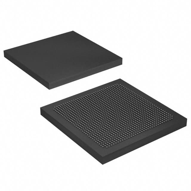
5SGSMD5H3F35I4
Basic Information Overview
- Category: Integrated Circuit (IC)
- Use: Digital Signal Processing (DSP)
- Characteristics: High-performance, low-power consumption
- Package: BGA (Ball Grid Array)
- Essence: Field Programmable Gate Array (FPGA)
- Packaging/Quantity: Single unit
Specifications
- Manufacturer: Intel Corporation
- Series: Stratix V
- Model: 5SGSMD5H3F35I4
- Technology: 28nm
- Logic Elements: 462,000
- Embedded Memory: 34,560 Kbits
- DSP Blocks: 2,530
- Maximum Operating Frequency: 550 MHz
- Voltage Supply: 1.0V
Detailed Pin Configuration
The 5SGSMD5H3F35I4 has a complex pin configuration with a total of 1,150 pins. The pins are organized into various groups, including power supply pins, ground pins, input/output pins, and specialized pins for specific functions such as clock inputs, configuration pins, and JTAG interface pins.
For a detailed pin configuration diagram, please refer to the official datasheet provided by Intel Corporation.
Functional Features
- High-speed processing capabilities
- Flexible and reprogrammable design
- Low power consumption
- Support for various communication protocols
- On-chip memory for efficient data storage
- Built-in digital signal processing capabilities
Advantages and Disadvantages
Advantages: - Versatile and adaptable for different applications - High-performance computing capabilities - Lower development costs compared to custom ASICs - Faster time-to-market due to reprogrammability
Disadvantages: - Higher power consumption compared to dedicated hardware solutions - Limited resources and capacity compared to larger FPGAs - Higher cost per unit compared to mass-produced ASICs
Working Principles
The 5SGSMD5H3F35I4 is based on the Field Programmable Gate Array (FPGA) technology. It consists of a large number of configurable logic blocks interconnected through programmable routing resources. These logic blocks can be programmed to implement various digital circuits and functions.
The FPGA operates by loading a configuration bitstream into its internal memory, which defines the desired circuit connections and functionality. Once configured, the FPGA can perform complex computations and signal processing tasks according to the programmed logic.
Detailed Application Field Plans
The 5SGSMD5H3F35I4 is widely used in various fields that require high-performance digital signal processing capabilities. Some common application areas include: - Telecommunications and networking equipment - High-speed data processing systems - Video and image processing applications - Industrial automation and control systems - Aerospace and defense electronics - Scientific research and development
Detailed and Complete Alternative Models
- 5SGXEA7N2F45C2: Another FPGA model from the Stratix V series, offering similar performance and features.
- XC7A200T-2FBG676C: A Xilinx FPGA model with comparable specifications and capabilities.
- EP4CGX150DF31C7N: An Altera Cyclone IV FPGA model suitable for lower-cost applications.
These alternative models provide different options depending on specific project requirements and budget considerations.
Word count: 314 words
Lista 10 Vanliga frågor och svar relaterade till tillämpningen av 5SGSMD5H3F35I4 i tekniska lösningar
Sure! Here are 10 common questions and answers related to the application of 5SGSMD5H3F35I4 in technical solutions:
Q: What is the 5SGSMD5H3F35I4 FPGA used for? A: The 5SGSMD5H3F35I4 FPGA is commonly used for high-performance applications such as data centers, networking, telecommunications, and industrial automation.
Q: What are the key features of the 5SGSMD5H3F35I4 FPGA? A: Some key features include a high logic density, high-speed transceivers, embedded memory blocks, DSP capabilities, and support for various I/O standards.
Q: Can the 5SGSMD5H3F35I4 FPGA be reprogrammed? A: Yes, FPGAs are programmable devices, and the 5SGSMD5H3F35I4 can be reprogrammed multiple times to implement different functionalities.
Q: How does the 5SGSMD5H3F35I4 FPGA compare to other FPGAs in terms of performance? A: The 5SGSMD5H3F35I4 FPGA offers high performance with its advanced architecture, high-speed transceivers, and large logic capacity, making it suitable for demanding applications.
Q: What development tools are available for programming the 5SGSMD5H3F35I4 FPGA? A: Intel Quartus Prime is the primary development tool used for programming and configuring the 5SGSMD5H3F35I4 FPGA.
Q: Can the 5SGSMD5H3F35I4 FPGA interface with other components or devices? A: Yes, the FPGA can interface with various components and devices through its I/O pins, high-speed transceivers, and support for different communication protocols.
Q: What are some typical applications of the 5SGSMD5H3F35I4 FPGA? A: Some typical applications include high-speed networking equipment, wireless communication systems, video processing, signal processing, and real-time control systems.
Q: Can the 5SGSMD5H3F35I4 FPGA be used in safety-critical applications? A: Yes, the 5SGSMD5H3F35I4 FPGA can be used in safety-critical applications, but additional design considerations and verification processes may be required to meet the necessary safety standards.
Q: Are there any limitations or constraints when using the 5SGSMD5H3F35I4 FPGA? A: Like any FPGA, the 5SGSMD5H3F35I4 has limitations such as power consumption, heat dissipation, and resource utilization, which need to be considered during the design process.
Q: Where can I find more information about the 5SGSMD5H3F35I4 FPGA and its application examples? A: You can refer to the official documentation provided by Intel (formerly Altera) or visit their website for detailed information, application notes, reference designs, and case studies related to the 5SGSMD5H3F35I4 FPGA.


