

5SGSMD3H1F35C2N
Product Overview
Category: Integrated Circuit (IC)
Use: The 5SGSMD3H1F35C2N is a high-performance field-programmable gate array (FPGA) designed for various applications in the electronics industry. It offers flexible programmability and high-speed processing capabilities.
Characteristics: - High-performance FPGA - Flexible programmability - High-speed processing - Versatile application possibilities
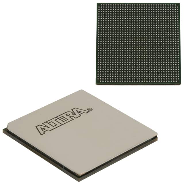
Package: The 5SGSMD3H1F35C2N comes in a compact and durable package, ensuring protection during transportation and handling. The package is designed to withstand various environmental conditions.
Essence: The essence of the 5SGSMD3H1F35C2N lies in its ability to provide a customizable and powerful solution for electronic systems. It enables designers to implement complex logic functions and algorithms efficiently.
Packaging/Quantity: The 5SGSMD3H1F35C2N is typically packaged individually in an anti-static bag to prevent electrostatic damage. It is available in various quantities depending on the requirements of the customer.
Specifications
- Model: 5SGSMD3H1F35C2N
- Technology: Field-Programmable Gate Array (FPGA)
- Logic Elements: 220,000
- Embedded Memory: 8,000 Kbits
- Maximum Operating Frequency: 500 MHz
- I/O Pins: 622
- Power Supply Voltage: 1.2V
- Package Type: BGA (Ball Grid Array)
- Package Dimensions: 35mm x 35mm
Detailed Pin Configuration
The 5SGSMD3H1F35C2N has a comprehensive pin configuration that allows for seamless integration into electronic systems. Here are some of the key pin functions:
- VCCINT: Power supply for internal logic circuits.
- VCCAUX: Auxiliary power supply for I/O banks and other components.
- GND: Ground connection for the device.
- CLK_IN: Input clock signal for synchronization.
- I/O Pins: Bidirectional pins for input/output data transfer.
- Configuration Pins: Pins used for device configuration.
For a complete and detailed pin configuration, please refer to the product datasheet.
Functional Features
The 5SGSMD3H1F35C2N offers several functional features that make it a versatile FPGA solution:
- High-Speed Processing: The FPGA operates at a maximum frequency of 500 MHz, enabling rapid data processing and real-time applications.
- Flexible Programmability: The device can be programmed and reprogrammed to implement various logic functions and algorithms, providing flexibility in system design.
- Embedded Memory: With 8,000 Kbits of embedded memory, the FPGA can store and process large amounts of data efficiently.
- Versatile I/O Capabilities: The 5SGSMD3H1F35C2N provides 622 bidirectional I/O pins, allowing for seamless integration with external devices and peripherals.
Advantages and Disadvantages
Advantages: - High-performance FPGA with flexible programmability - Versatile application possibilities - Large embedded memory capacity - Extensive I/O capabilities
Disadvantages: - Relatively high power consumption compared to other low-power alternatives - Requires expertise in FPGA programming for optimal utilization
Working Principles
The 5SGSMD3H1F35C2N operates based on the principles of field-programmable gate arrays. It consists of an array of configurable logic blocks (CLBs) interconnected through programmable interconnects. These CLBs can be programmed to implement various logic functions, allowing for the creation of complex digital circuits.
The device is programmed using a hardware description language (HDL) such as VHDL or Verilog. The programming code describes the desired logic functions and connections within the FPGA. Once programmed, the FPGA can execute these functions in real-time.
Detailed Application Field Plans
The 5SGSMD3H1F35C2N finds applications in various fields, including:
- Communications: The FPGA can be used in communication systems for signal processing, protocol implementation, and data encryption.
- Industrial Automation: It enables the development of advanced control systems, robotics, and machine vision applications.
- Medical Electronics: The FPGA can be utilized in medical imaging, patient monitoring, and diagnostic equipment.
- Aerospace and Defense: It finds applications in radar systems, avionics, and secure communications.
- High-Performance Computing: The FPGA can accelerate computationally intensive tasks in scientific research, financial modeling, and artificial intelligence.
These are just a few examples, and the versatility of the 5SGSMD3H1F
Lista 10 Vanliga frågor och svar relaterade till tillämpningen av 5SGSMD3H1F35C2N i tekniska lösningar
Sure! Here are 10 common questions and answers related to the application of 5SGSMD3H1F35C2N in technical solutions:
Q1: What is the 5SGSMD3H1F35C2N? A1: The 5SGSMD3H1F35C2N is a specific model of Field-Programmable Gate Array (FPGA) manufactured by Intel.
Q2: What are the key features of the 5SGSMD3H1F35C2N? A2: The 5SGSMD3H1F35C2N offers high-performance processing capabilities, low power consumption, large capacity for logic elements, and various I/O interfaces.
Q3: In what technical solutions can the 5SGSMD3H1F35C2N be used? A3: The 5SGSMD3H1F35C2N can be utilized in a wide range of applications such as telecommunications, data centers, industrial automation, aerospace, and defense.
Q4: How does the 5SGSMD3H1F35C2N contribute to improving performance in technical solutions? A4: The 5SGSMD3H1F35C2N provides high-speed processing capabilities, parallel computing, and customizable hardware acceleration, which can significantly enhance system performance.
Q5: Can the 5SGSMD3H1F35C2N be programmed or reconfigured? A5: Yes, the 5SGSMD3H1F35C2N is a Field-Programmable Gate Array, meaning it can be programmed and reconfigured to implement different functionalities based on specific requirements.
Q6: What programming languages can be used with the 5SGSMD3H1F35C2N? A6: The 5SGSMD3H1F35C2N can be programmed using hardware description languages (HDLs) such as VHDL or Verilog, as well as high-level synthesis tools like OpenCL.
Q7: Are there any development tools available for working with the 5SGSMD3H1F35C2N? A7: Yes, Intel provides Quartus Prime software suite, which includes design tools, simulation environments, and programming interfaces specifically tailored for FPGA development, including the 5SGSMD3H1F35C2N.
Q8: Can the 5SGSMD3H1F35C2N interface with other components or devices? A8: Yes, the 5SGSMD3H1F35C2N supports various I/O standards and interfaces, including PCIe, Ethernet, USB, DDR memory, and more, allowing seamless integration with other components and devices.
Q9: What are the power requirements for the 5SGSMD3H1F35C2N? A9: The power requirements for the 5SGSMD3H1F35C2N depend on the specific implementation and configuration. It is recommended to refer to the datasheet and design guidelines provided by Intel for accurate power estimation.
Q10: Where can I find additional resources and support for working with the 5SGSMD3H1F35C2N? A10: Intel's website offers comprehensive documentation, application notes, reference designs, and a community forum dedicated to FPGA development, which can provide valuable resources and support for working with the 5SGSMD3H1F35C2N.