

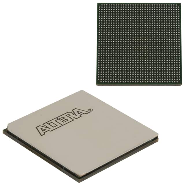
5CGXFC9E7F35C8N
Product Overview
Category
The 5CGXFC9E7F35C8N belongs to the category of Field Programmable Gate Arrays (FPGAs).
Use
FPGAs are integrated circuits that can be programmed and reprogrammed to perform various digital functions. The 5CGXFC9E7F35C8N is specifically designed for high-performance applications that require complex logic functions.
Characteristics
- High-performance FPGA with advanced features
- Large number of programmable logic elements
- High-speed transceivers for data communication
- On-chip memory resources
- Flexible I/O interfaces
- Low power consumption
Package
The 5CGXFC9E7F35C8N is available in a compact package that ensures easy integration into electronic systems. It is designed to be mounted on a printed circuit board (PCB) using surface mount technology (SMT).
Essence
The essence of the 5CGXFC9E7F35C8N lies in its ability to provide a highly configurable and flexible platform for implementing complex digital designs. Its programmability allows for rapid prototyping and customization, making it suitable for a wide range of applications.
Packaging/Quantity
The 5CGXFC9E7F35C8N is typically sold in reels or trays, depending on the manufacturer's packaging standards. The quantity per package may vary, but it is commonly available in quantities of 100 or more.
Specifications
- Logic Elements: 9,150
- Embedded Memory: 1,638 Kbits
- Transceivers: 24
- Maximum Operating Frequency: 500 MHz
- Operating Voltage: 1.2V
- Package Type: F35 (35mm x 35mm)
Detailed Pin Configuration
The 5CGXFC9E7F35C8N has a complex pin configuration with multiple I/O banks, power supply pins, and configuration pins. For detailed information on the pin configuration, please refer to the manufacturer's datasheet.
Functional Features
- High-speed data processing capabilities
- Support for various communication protocols
- On-chip memory resources for efficient data storage
- Flexible I/O interfaces for easy integration with external devices
- Configurable logic elements for implementing complex digital functions
- Low power consumption for energy-efficient operation
Advantages and Disadvantages
Advantages
- High performance and flexibility
- Rapid prototyping and customization
- Wide range of application possibilities
- Efficient use of resources
- Energy-efficient operation
Disadvantages
- Steep learning curve for beginners
- Higher cost compared to other programmable logic devices
- Limited availability of alternative models
Working Principles
The 5CGXFC9E7F35C8N operates based on the principles of reconfigurable computing. It consists of an array of programmable logic elements interconnected by configurable routing resources. The device can be programmed using hardware description languages (HDL) or graphical tools to define the desired functionality. Once programmed, the FPGA executes the specified digital functions by routing signals through the configured logic elements.
Detailed Application Field Plans
The 5CGXFC9E7F35C8N finds applications in various fields, including:
- Telecommunications: Used in high-speed data communication systems, network routers, and switches.
- Aerospace and Defense: Employed in radar systems, avionics, and military communication equipment.
- Industrial Automation: Utilized in control systems, robotics, and machine vision applications.
- Medical Devices: Integrated into medical imaging systems, patient monitoring devices, and diagnostic equipment.
- Automotive: Applied in advanced driver-assistance systems (ADAS), infotainment systems, and engine control units.
Detailed and Complete Alternative Models
While the 5CGXFC9E7F35C8N offers advanced features and performance, there are alternative FPGA models available in the market. Some notable alternatives include:
- Xilinx Virtex UltraScale+: Offers higher logic capacity and faster transceivers.
- Intel Stratix 10: Provides advanced security features and high-speed interfaces.
- Lattice ECP5: Focuses on low power consumption and small form factor applications.
These alternative models cater to specific requirements and offer different trade-offs in terms of performance, power consumption, and cost.
In conclusion, the 5CGXFC9E7F35C8N is a high-performance FPGA that provides flexibility, configurability, and advanced features for implementing complex digital designs. Its wide range of applications, efficient resource utilization, and energy-efficient operation make it a valuable component in various industries.
Lista 10 Vanliga frågor och svar relaterade till tillämpningen av 5CGXFC9E7F35C8N i tekniska lösningar
Sure! Here are 10 common questions and answers related to the application of 5CGXFC9E7F35C8N in technical solutions:
Q: What is the 5CGXFC9E7F35C8N? A: The 5CGXFC9E7F35C8N is a field-programmable gate array (FPGA) manufactured by Intel. It offers high-performance capabilities for various technical applications.
Q: What are the key features of the 5CGXFC9E7F35C8N? A: The key features include 9,024 logic elements, 414,720 adaptive logic modules, 1,152 embedded memory blocks, and support for various I/O standards.
Q: What are some typical applications of the 5CGXFC9E7F35C8N? A: The 5CGXFC9E7F35C8N can be used in applications such as telecommunications, industrial automation, automotive electronics, medical devices, and high-performance computing.
Q: How can I program the 5CGXFC9E7F35C8N? A: You can program the 5CGXFC9E7F35C8N using Intel's Quartus Prime software, which provides a user-friendly interface for designing, simulating, and programming the FPGA.
Q: Can the 5CGXFC9E7F35C8N interface with other components or devices? A: Yes, the 5CGXFC9E7F35C8N supports various communication protocols such as PCIe, Ethernet, USB, and DDR3 memory interfaces, allowing it to interface with other components or devices.
Q: What kind of performance can I expect from the 5CGXFC9E7F35C8N? A: The 5CGXFC9E7F35C8N offers high-performance capabilities, including fast logic processing, high-speed data transfer, and low-latency communication.
Q: Can the 5CGXFC9E7F35C8N be used for real-time signal processing? A: Yes, the 5CGXFC9E7F35C8N is well-suited for real-time signal processing applications due to its high-speed processing capabilities and support for various digital signal processing (DSP) functions.
Q: Is the 5CGXFC9E7F35C8N suitable for power-constrained applications? A: Yes, the 5CGXFC9E7F35C8N offers power optimization features such as dynamic power management and clock gating, making it suitable for power-constrained applications.
Q: Can the 5CGXFC9E7F35C8N be reprogrammed multiple times? A: Yes, the 5CGXFC9E7F35C8N is a reprogrammable FPGA, allowing you to modify and reconfigure its functionality multiple times during the development or deployment phase.
Q: Where can I find additional resources and support for the 5CGXFC9E7F35C8N? A: You can find additional resources, documentation, and technical support for the 5CGXFC9E7F35C8N on Intel's official website or through their customer support channels.