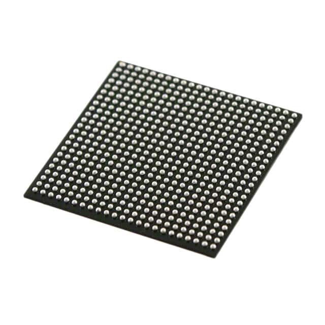
5CEBA5U19C8N
Product Overview
Category
The 5CEBA5U19C8N belongs to the category of Field Programmable Gate Arrays (FPGAs).
Use
This FPGA is commonly used in various electronic devices and systems for digital logic implementation, such as communication equipment, industrial control systems, and consumer electronics.
Characteristics
- High flexibility: The 5CEBA5U19C8N offers a high level of programmability, allowing users to configure the device according to their specific requirements.
- High performance: With its advanced architecture and optimized circuitry, this FPGA delivers fast processing speeds and efficient resource utilization.
- Low power consumption: The 5CEBA5U19C8N is designed to minimize power consumption, making it suitable for battery-powered applications.
- Large capacity: This FPGA provides a generous amount of programmable logic elements, memory blocks, and I/O pins, enabling the implementation of complex designs.
Package
The 5CEBA5U19C8N is available in a compact and durable package, ensuring easy integration into various electronic systems. It is typically offered in a surface-mount package, allowing for efficient PCB assembly.
Essence
The essence of the 5CEBA5U19C8N lies in its ability to provide a reconfigurable hardware platform that can be customized to meet specific application requirements. It serves as a versatile solution for implementing complex digital logic functions.
Packaging/Quantity
The 5CEBA5U19C8N is usually supplied in reels or trays, depending on the manufacturer's packaging standards. The quantity per package may vary, but it is commonly available in quantities of 100 or more.
Specifications
- Logic Elements: 5,120
- Memory Blocks: 288
- Embedded Multipliers: 36
- Maximum Operating Frequency: 400 MHz
- I/O Pins: 266
- Operating Voltage: 1.2V
Detailed Pin Configuration
The 5CEBA5U19C8N has a comprehensive pin configuration, enabling connectivity with external components and systems. The detailed pinout can be found in the device's datasheet.
Functional Features
High-Level Programmability
The 5CEBA5U19C8N offers a wide range of programmable features, including logic functions, memory configurations, and I/O standards. This allows designers to tailor the FPGA to their specific application requirements.
Advanced Clock Management
This FPGA incorporates advanced clock management circuitry, providing precise control over clock signals. It supports various clocking options, such as PLLs (Phase-Locked Loops) and DLLs (Delay-Locked Loops), ensuring reliable timing synchronization within the system.
Flexible I/O Interfaces
The 5CEBA5U19C8N provides a variety of I/O standards, including LVCMOS, LVTTL, and differential signaling standards like LVDS and LVPECL. This flexibility enables seamless integration with different external devices and interfaces.
Embedded Memory Blocks
With its embedded memory blocks, the 5CEBA5U19C8N facilitates efficient implementation of data storage and processing functions. These memory blocks can be configured as RAM, ROM, FIFO buffers, or other custom memory structures.
Advantages and Disadvantages
Advantages
- High flexibility and reconfigurability
- Excellent performance and resource utilization
- Low power consumption
- Large capacity for complex designs
- Wide range of I/O standards
Disadvantages
- Steeper learning curve compared to fixed-function ASICs
- Higher cost per unit compared to mass-produced standard ICs
- Limited availability of alternative models from different manufacturers
Working Principles
The 5CEBA5U19C8N operates based on the principles of reconfigurable computing. It consists of an array of programmable logic elements interconnected through configurable routing resources. The device can be programmed using Hardware Description Languages (HDLs) like VHDL or Verilog, which describe the desired digital logic functionality. Upon programming, the FPGA's internal configuration memory is loaded, establishing the desired circuit connections and behavior.
Detailed Application Field Plans
The 5CEBA5U19C8N finds applications in various fields, including:
- Communication Systems: Used for protocol processing, encryption/decryption, and signal modulation/demodulation.
- Industrial Control Systems: Employed for real-time control, data acquisition, and monitoring in manufacturing and automation processes.
- Consumer Electronics: Integrated into devices like high-definition televisions, gaming consoles, and audio/video processing systems.
- Medical Equipment: Utilized for image processing, patient monitoring, and diagnostic systems.
- Aerospace and Defense: Applied in radar systems, avionics, and secure communication equipment.
Alternative Models
While the 5CEBA5U19C8N
Lista 10 Vanliga frågor och svar relaterade till tillämpningen av 5CEBA5U19C8N i tekniska lösningar
Sure! Here are 10 common questions and answers related to the application of 5CEBA5U19C8N in technical solutions:
Q: What is 5CEBA5U19C8N? A: 5CEBA5U19C8N is a field-programmable gate array (FPGA) chip manufactured by Intel.
Q: What are the key features of 5CEBA5U19C8N? A: Some key features include 5,120 logic elements, 266 user I/O pins, embedded memory blocks, and support for various communication protocols.
Q: How can 5CEBA5U19C8N be used in technical solutions? A: It can be used to implement complex digital logic designs, accelerate data processing, perform high-speed signal processing, and enable hardware acceleration in various applications.
Q: What programming languages are supported for programming 5CEBA5U19C8N? A: 5CEBA5U19C8N can be programmed using Hardware Description Languages (HDLs) such as VHDL or Verilog.
Q: Can 5CEBA5U19C8N be reprogrammed after deployment? A: Yes, 5CEBA5U19C8N is a reprogrammable FPGA, allowing for flexibility and iterative development.
Q: What are some typical applications of 5CEBA5U19C8N? A: It can be used in areas like telecommunications, aerospace, automotive, industrial automation, image and video processing, and scientific research.
Q: Does 5CEBA5U19C8N require any additional components for integration into a system? A: Yes, it may require external components such as power supply, clock source, and configuration memory for proper integration.
Q: What are the advantages of using 5CEBA5U19C8N over traditional microcontrollers or ASICs? A: FPGA chips like 5CEBA5U19C8N offer higher flexibility, faster development cycles, lower non-recurring engineering costs, and the ability to implement custom logic functions.
Q: Are there any limitations or challenges when working with 5CEBA5U19C8N? A: Some challenges include longer design cycles, higher power consumption compared to microcontrollers, and a steeper learning curve for programming and optimization.
Q: Where can I find resources and support for working with 5CEBA5U19C8N? A: Intel provides documentation, reference designs, development tools, and an online community for support. Additionally, there are various online forums and tutorials available for FPGA programming in general.
Please note that the specific details and answers may vary depending on the context and requirements of the technical solution.


