

5AGXFB7H4F35I5
Basic Information Overview
- Category: Integrated Circuit (IC)
- Use: Programmable Logic Device (PLD)
- Characteristics: High-performance, low-power consumption, reprogrammable
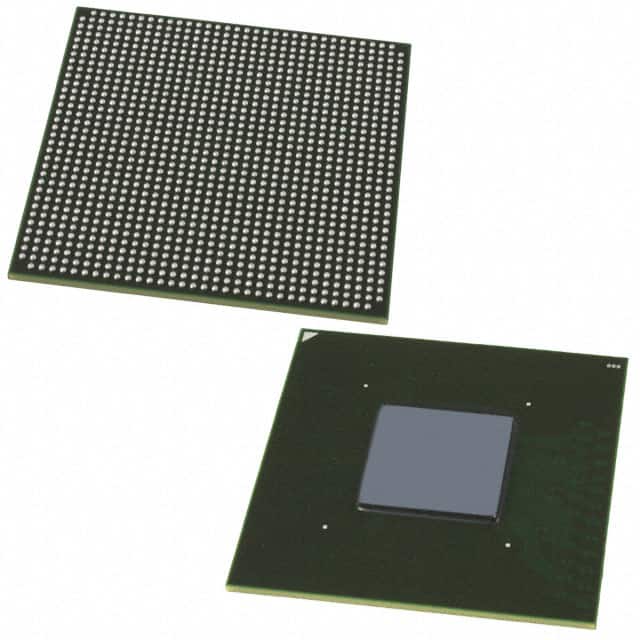
- Package: BGA (Ball Grid Array)
- Essence: FPGA (Field-Programmable Gate Array)
- Packaging/Quantity: Single unit
Specifications
- Model: 5AGXFB7H4F35I5
- Technology: 28nm
- Logic Elements: 768,000
- Embedded Memory: 27,648 Kbits
- DSP Blocks: 1,920
- Maximum User I/Os: 840
- Operating Voltage: 1.2V
- Speed Grade: -5
Detailed Pin Configuration
The 5AGXFB7H4F35I5 has a complex pin configuration with multiple pins dedicated to various functions. The detailed pin configuration can be found in the datasheet provided by the manufacturer.
Functional Features
- High-performance processing capabilities
- Low power consumption
- Reprogrammable design allows for flexibility and adaptability
- Large number of logic elements and embedded memory for complex designs
- Abundant DSP blocks for signal processing applications
- Wide range of user I/Os for interfacing with external devices
Advantages
- Versatile and flexible due to its reprogrammable nature
- High-performance processing capabilities suitable for demanding applications
- Low power consumption helps reduce energy costs
- Ample logic elements and embedded memory enable complex designs
- Abundant DSP blocks facilitate efficient signal processing
- Extensive user I/Os provide connectivity options
Disadvantages
- Relatively high cost compared to fixed-function integrated circuits
- Steeper learning curve for programming and utilizing the device's full potential
- Limited availability of alternative models due to its specific specifications
Working Principles
The 5AGXFB7H4F35I5 is based on FPGA technology, which allows users to configure the device according to their specific requirements. It consists of an array of programmable logic elements interconnected through configurable routing resources. These logic elements can be programmed to perform various functions and create complex digital circuits. The device's configuration is stored in non-volatile memory, allowing it to retain the programmed design even after power is removed.
Detailed Application Field Plans
- Digital signal processing
- High-speed data communication
- Industrial automation
- Aerospace and defense systems
- Video and image processing
- Embedded systems
Detailed and Complete Alternative Models
- 5AGXFB3H4F35I5
- 5AGXFB5H4F35I5
- 5AGXFB9H4F35I5
- 5AGXFB12H4F35I5
- 5AGXFB15H4F35I5
These alternative models offer similar functionality and characteristics but may differ in terms of logic elements, embedded memory, or I/O count.
Note: The above content provides a brief overview of the requested information. Additional details and specifications can be found in the datasheet provided by the manufacturer.
Lista 10 Vanliga frågor och svar relaterade till tillämpningen av 5AGXFB7H4F35I5 i tekniska lösningar
Sure! Here are 10 common questions and answers related to the application of 5AGXFB7H4F35I5 in technical solutions:
Q: What is the 5AGXFB7H4F35I5 FPGA used for? A: The 5AGXFB7H4F35I5 FPGA is a Field-Programmable Gate Array that can be used for various applications such as high-performance computing, networking, and industrial automation.
Q: What are the key features of the 5AGXFB7H4F35I5 FPGA? A: Some key features of this FPGA include high logic density, low power consumption, high-speed transceivers, embedded memory blocks, and support for various I/O standards.
Q: Can the 5AGXFB7H4F35I5 FPGA be reprogrammed? A: Yes, the 5AGXFB7H4F35I5 FPGA is field-programmable, meaning it can be reprogrammed multiple times to implement different functionalities or adapt to changing requirements.
Q: What development tools are available for programming the 5AGXFB7H4F35I5 FPGA? A: Intel Quartus Prime is the primary development tool used for programming and configuring the 5AGXFB7H4F35I5 FPGA. It provides a comprehensive suite of design and verification tools.
Q: What interfaces does the 5AGXFB7H4F35I5 FPGA support? A: The 5AGXFB7H4F35I5 FPGA supports various interfaces such as PCIe, Ethernet, USB, DDR3/DDR4 memory, HDMI, and many more, making it versatile for different applications.
Q: Can the 5AGXFB7H4F35I5 FPGA handle high-speed data processing? A: Yes, the 5AGXFB7H4F35I5 FPGA is equipped with high-speed transceivers that can handle data rates up to several gigabits per second, making it suitable for high-speed data processing applications.
Q: What are some typical applications of the 5AGXFB7H4F35I5 FPGA? A: Some typical applications include software-defined networking (SDN), wireless communication systems, video processing, image recognition, and real-time signal processing.
Q: Can the 5AGXFB7H4F35I5 FPGA be used in safety-critical systems? A: Yes, the 5AGXFB7H4F35I5 FPGA can be used in safety-critical systems. However, additional measures such as redundancy and fault-tolerant design should be implemented to ensure reliability.
Q: Are there any limitations or considerations when using the 5AGXFB7H4F35I5 FPGA? A: Like any FPGA, the 5AGXFB7H4F35I5 has limitations such as limited resources, power consumption, and complexity of design. It's important to carefully plan and optimize your design to meet these constraints.
Q: Where can I find more information about the 5AGXFB7H4F35I5 FPGA? A: You can find more detailed information about the 5AGXFB7H4F35I5 FPGA, including datasheets, user guides, and application notes, on the official Intel website or by contacting their support team.
Please note that the specific details and answers may vary depending on the actual specifications and documentation provided by the manufacturer.