

5AGXBA1D4F31C5N
Product Overview
Category
The 5AGXBA1D4F31C5N belongs to the category of Field Programmable Gate Arrays (FPGAs).
Use
FPGAs are integrated circuits that can be programmed after manufacturing, allowing for flexible and customizable digital logic designs. The 5AGXBA1D4F31C5N is specifically designed for high-performance applications.
Characteristics
- High-performance FPGA with advanced features
- Large capacity for complex designs
- Low power consumption
- High-speed data processing capabilities
- Flexible and reconfigurable architecture
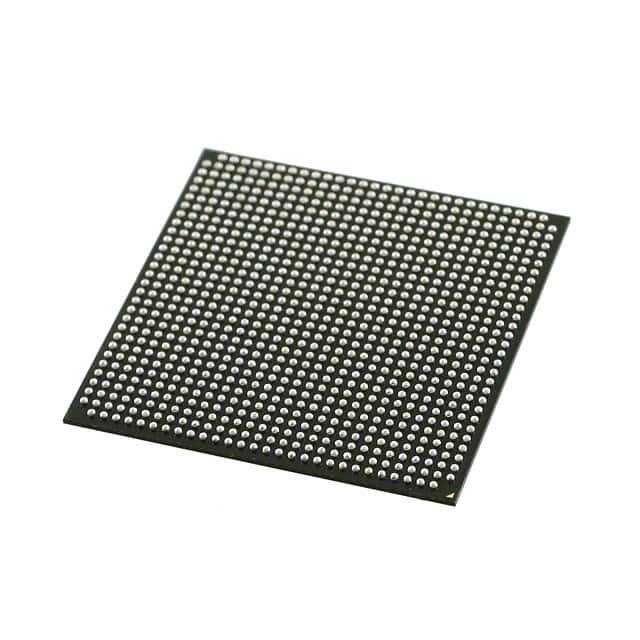
Package
The 5AGXBA1D4F31C5N comes in a compact package suitable for surface mount technology (SMT) assembly. It is available in a variety of package options, including ball grid array (BGA) and quad flat no-leads (QFN).
Essence
The essence of the 5AGXBA1D4F31C5N lies in its ability to provide designers with a versatile platform for implementing complex digital systems. Its programmability allows for rapid prototyping and iterative design processes.
Packaging/Quantity
The 5AGXBA1D4F31C5N is typically sold in reels or trays, depending on the chosen package type. The quantity per reel or tray may vary, but it is commonly available in quantities of 100 or more.
Specifications
- Logic Elements: 115,200
- Embedded Memory: Up to 10,368 Kbits
- DSP Blocks: 360
- Maximum User I/Os: 1,080
- Operating Voltage: 1.2V
- Operating Temperature Range: -40°C to 100°C
- Package Options: BGA, QFN
Detailed Pin Configuration
The 5AGXBA1D4F31C5N has a complex pin configuration with multiple I/O banks, power supply pins, and configuration pins. For a detailed pinout diagram and description, please refer to the manufacturer's datasheet.
Functional Features
- High-speed serial transceivers for high-bandwidth data communication
- Dedicated digital signal processing (DSP) blocks for efficient mathematical operations
- On-chip memory resources for data storage and retrieval
- Flexible clock management resources for precise timing control
- Support for various communication protocols, such as PCIe, Ethernet, and USB
Advantages and Disadvantages
Advantages
- Flexibility: The FPGA's programmability allows for customization and adaptation to specific application requirements.
- Performance: The 5AGXBA1D4F31C5N offers high-performance capabilities suitable for demanding applications.
- Reconfigurability: Design changes can be implemented by reprogramming the FPGA, eliminating the need for hardware modifications.
Disadvantages
- Complexity: Utilizing FPGAs requires expertise in digital design and programming.
- Cost: FPGAs can be more expensive than fixed-function integrated circuits due to their flexibility and advanced features.
- Power Consumption: FPGAs typically consume more power compared to dedicated ASICs or microcontrollers.
Working Principles
FPGAs consist of an array of configurable logic blocks interconnected through programmable routing resources. These logic blocks can be programmed to implement desired digital functions using a hardware description language (HDL). Upon programming, the FPGA's internal connections are established, allowing it to perform the specified logic operations.
Detailed Application Field Plans
The 5AGXBA1D4F31C5N finds applications in various fields, including:
- Telecommunications: Used in base stations, routers, and network switches for high-speed data processing and protocol handling.
- Aerospace and Defense: Employed in radar systems, avionics, and military communication equipment for their high-performance and reconfigurable nature.
- Industrial Automation: Utilized in control systems, robotics, and machine vision applications to implement complex algorithms and real-time data processing.
- Medical Devices: Used in medical imaging, patient monitoring, and diagnostic equipment for their ability to handle large amounts of data and perform complex calculations.
Detailed and Complete Alternative Models
- 5AGXBA1D4F31C6N: Similar to the 5AGXBA1D4F31C5N but with increased logic capacity and additional features.
- 5AGXBA1D4F31C4N: A lower-cost variant with reduced logic capacity but suitable for less demanding applications.
- 5AGXBA1D4F31C7N: An enhanced version with higher performance and additional I/O capabilities.
These alternative models provide designers with options that cater to different project requirements and budgets.
In conclusion, the 5AGXBA1D4F31C5N is a high-performance FPGA offering flexibility,
Lista 10 Vanliga frågor och svar relaterade till tillämpningen av 5AGXBA1D4F31C5N i tekniska lösningar
Sure! Here are 10 common questions and answers related to the application of 5AGXBA1D4F31C5N in technical solutions:
Q1: What is the 5AGXBA1D4F31C5N? A1: The 5AGXBA1D4F31C5N is a specific model of Field-Programmable Gate Array (FPGA) manufactured by Intel.
Q2: What are the key features of the 5AGXBA1D4F31C5N? A2: The 5AGXBA1D4F31C5N offers high-performance processing capabilities, low power consumption, large capacity for logic elements, and support for various I/O interfaces.
Q3: In what technical solutions can the 5AGXBA1D4F31C5N be used? A3: The 5AGXBA1D4F31C5N can be used in a wide range of applications such as telecommunications, industrial automation, automotive electronics, aerospace, and defense systems.
Q4: How can the 5AGXBA1D4F31C5N be programmed? A4: The 5AGXBA1D4F31C5N can be programmed using Hardware Description Languages (HDLs) like VHDL or Verilog, or through graphical programming tools provided by Intel.
Q5: What advantages does the 5AGXBA1D4F31C5N offer over traditional microcontrollers? A5: The 5AGXBA1D4F31C5N provides greater flexibility and scalability compared to traditional microcontrollers. It allows for custom hardware implementation, parallel processing, and faster execution of complex algorithms.
Q6: Can the 5AGXBA1D4F31C5N interface with other components or devices? A6: Yes, the 5AGXBA1D4F31C5N supports various I/O interfaces such as UART, SPI, I2C, Ethernet, and PCIe, enabling seamless integration with other components or devices.
Q7: What is the power consumption of the 5AGXBA1D4F31C5N? A7: The power consumption of the 5AGXBA1D4F31C5N depends on the specific design and configuration. However, it is generally known for its low power consumption compared to alternative solutions.
Q8: Can the 5AGXBA1D4F31C5N be reprogrammed after deployment? A8: Yes, the 5AGXBA1D4F31C5N is a reprogrammable FPGA, allowing for updates and modifications to the implemented logic even after deployment.
Q9: Are there any development tools available for programming the 5AGXBA1D4F31C5N? A9: Yes, Intel provides Quartus Prime software suite, which includes tools for designing, simulating, and programming the 5AGXBA1D4F31C5N.
Q10: Where can I find additional resources and support for working with the 5AGXBA1D4F31C5N? A10: Intel's website offers comprehensive documentation, application notes, reference designs, and an active community forum where you can find additional resources and support for working with the 5AGXBA1D4F31C5N.