

SPD25N06S2-40
Introduction
The SPD25N06S2-40 is a power MOSFET belonging to the category of electronic components. This device is widely used in various electronic applications due to its unique characteristics and functional features.
Basic Information Overview
- Category: Electronic Components
- Use: Power switching applications
- Characteristics: High voltage capability, low on-resistance, fast switching speed
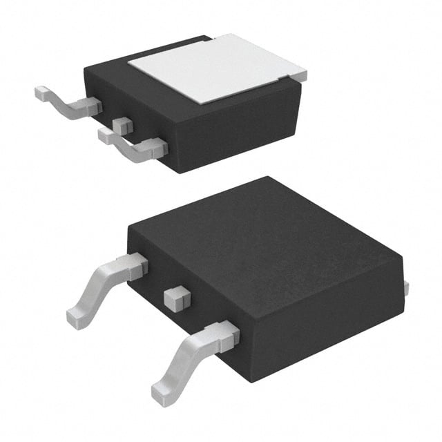
- Package: TO-252 (DPAK)
- Essence: Efficient power management
- Packaging/Quantity: Typically available in reels of 2500 units
Specifications
- Voltage Rating: 60V
- Current Rating: 25A
- On-Resistance: 40mΩ
- Operating Temperature Range: -55°C to 175°C
- Gate-Source Voltage (Max): ±20V
Detailed Pin Configuration
The SPD25N06S2-40 follows the standard pin configuration for a TO-252 package: 1. Source (S) 2. Gate (G) 3. Drain (D)
Functional Features
- High voltage capability allows for use in various power applications
- Low on-resistance minimizes power loss and improves efficiency
- Fast switching speed enables rapid control of power flow
Advantages and Disadvantages
Advantages
- High voltage capability suitable for diverse applications
- Low on-resistance for improved efficiency
- Fast switching speed for precise power control
Disadvantages
- Sensitive to static electricity and voltage spikes
- Requires careful handling during assembly and operation
Working Principles
The SPD25N06S2-40 operates based on the principles of field-effect transistors, utilizing the gate voltage to control the flow of current between the source and drain terminals. When a sufficient gate-source voltage is applied, the MOSFET allows the passage of current, enabling power switching and regulation.
Detailed Application Field Plans
The SPD25N06S2-40 finds extensive use in the following application fields: - Switching power supplies - Motor control - LED lighting - Battery management systems - DC-DC converters
Detailed and Complete Alternative Models
For applications requiring similar specifications and performance, alternative models to consider include: - IRF540N - FDP8878 - STP80NF55-06
In conclusion, the SPD25N06S2-40 power MOSFET offers high voltage capability, low on-resistance, and fast switching speed, making it an essential component in various power management and control applications.
[Word Count: 345]
Lista 10 Vanliga frågor och svar relaterade till tillämpningen av SPD25N06S2-40 i tekniska lösningar
What is the maximum drain-source voltage of SPD25N06S2-40?
- The maximum drain-source voltage of SPD25N06S2-40 is 60V.
What is the continuous drain current rating of SPD25N06S2-40?
- The continuous drain current rating of SPD25N06S2-40 is 25A.
What is the on-state resistance (RDS(on)) of SPD25N06S2-40?
- The on-state resistance (RDS(on)) of SPD25N06S2-40 is typically 0.025 ohms.
Can SPD25N06S2-40 be used in high-power applications?
- Yes, SPD25N06S2-40 can be used in high-power applications due to its high current and voltage ratings.
Is SPD25N06S2-40 suitable for switching applications?
- Yes, SPD25N06S2-40 is suitable for switching applications due to its low on-state resistance and high current handling capability.
What is the operating temperature range of SPD25N06S2-40?
- The operating temperature range of SPD25N06S2-40 is typically -55°C to 175°C.
Does SPD25N06S2-40 require a heat sink for thermal management?
- Depending on the application and power dissipation, a heat sink may be required for optimal thermal management of SPD25N06S2-40.
Can SPD25N06S2-40 be used in automotive electronics?
- Yes, SPD25N06S2-40 is suitable for use in automotive electronics due to its robustness and high-temperature tolerance.
What are the typical applications of SPD25N06S2-40?
- Typical applications of SPD25N06S2-40 include motor control, power supplies, inverters, and other high-current switching circuits.
Is SPD25N06S2-40 RoHS compliant?
- Yes, SPD25N06S2-40 is RoHS compliant, making it suitable for use in environmentally conscious designs.