

IDT71V2546S133PFI8
Product Overview
- Category: Integrated Circuit (IC)
- Use: Memory device
- Characteristics: High-speed, low-power, synchronous static random-access memory (SRAM)
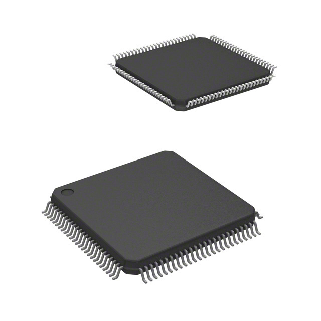
- Package: 208-pin plastic quad flat pack (PQFP)
- Essence: Provides fast and reliable data storage and retrieval capabilities
- Packaging/Quantity: Sold in reels, typically containing 250 units
Specifications
- Memory Type: Synchronous SRAM
- Density: 4 Megabits (256K x 16)
- Access Time: 133 nanoseconds
- Operating Voltage: 3.3 volts
- Operating Temperature Range: -40°C to +85°C
- Data Retention: Greater than 10 years
- Interface: Parallel
Pin Configuration
The IDT71V2546S133PFI8 has a total of 208 pins. The pin configuration is as follows:
- VDDQ
- DQ0
- DQ1
- DQ2
- DQ3
- DQ4
- DQ5
- DQ6
- DQ7
- VSSQ
- DQ8
- DQ9
- DQ10
- DQ11
- DQ12
- DQ13
- DQ14
- DQ15
- VDDQ
- A0
- A1
- A2
- A3
- A4
- A5
- A6
- A7
- A8
- A9
- A10
- A11
- A12
- A13
- A14
- A15
- VSSQ
- A16
- A17
- A18
- A19
- A20
- A21
- A22
- A23
- A24
- A25
- A26
- A27
- A28
- A29
- A30
- A31
- VDDQ
- WE#
- CAS#
- RAS#
- OE#
- UB#
- LB#
- CE2#
- CE1#
- CE0#
- VSSQ
- DQM0#
- DQM1#
- DQM2#
- DQM3#
- CLK
- CLKEN#
- CKE#
- CS#
- VDDQ
- NC
- NC
- NC
- NC
- NC
- NC
- NC
- NC
- NC
- NC
- NC
- NC
- NC
- NC
- NC
- NC
- VSSQ
- NC
- NC
- NC
- NC
- NC
- NC
- NC
- NC
- NC
- NC
- NC
- NC
- NC
- NC
- NC
- NC
- VDDQ
- NC
- NC
- NC
- NC
- NC
- NC
- NC
- NC
- NC
- NC
- NC
- NC
- NC
- NC
- NC
- NC
- VSSQ
- NC
- NC
- NC
- NC
- NC
- NC
- NC
- NC
- NC
- NC
- NC
- NC
- NC
- NC
- NC
- NC
- VDDQ
- NC
- NC
- NC
- NC
- NC
- NC
- NC
- NC
- NC
- NC
- NC
- NC
- NC
- NC
- NC
- NC
- VSSQ
- NC
- NC
- NC
- NC
- NC
- NC
- NC
- NC
- NC
- NC
- NC
- NC
- NC
- NC
Lista 10 Vanliga frågor och svar relaterade till tillämpningen av IDT71V2546S133PFI8 i tekniska lösningar
Sure! Here are 10 common questions and answers related to the application of IDT71V2546S133PFI8 in technical solutions:
Question: What is the IDT71V2546S133PFI8?
Answer: The IDT71V2546S133PFI8 is a synchronous SRAM (Static Random Access Memory) chip with a capacity of 256K x 18 bits.Question: What is the operating voltage range for this chip?
Answer: The IDT71V2546S133PFI8 operates at a voltage range of 3.0V to 3.6V.Question: What is the maximum clock frequency supported by this chip?
Answer: This chip supports a maximum clock frequency of 133 MHz.Question: Can I use this chip in battery-powered devices?
Answer: Yes, the IDT71V2546S133PFI8 can be used in battery-powered devices as it operates at low power consumption levels.Question: What is the access time of this chip?
Answer: The access time of the IDT71V2546S133PFI8 is 8 ns.Question: Is this chip compatible with other standard memory interfaces?
Answer: Yes, this chip is compatible with industry-standard memory interfaces such as asynchronous and synchronous interface standards.Question: Can I use multiple IDT71V2546S133PFI8 chips in parallel to increase memory capacity?
Answer: Yes, you can use multiple chips in parallel to increase the overall memory capacity in your system.Question: Does this chip support burst mode operation?
Answer: Yes, the IDT71V2546S133PFI8 supports burst mode operation, allowing for faster data transfer.Question: What is the package type of this chip?
Answer: The IDT71V2546S133PFI8 comes in a 100-pin TQFP (Thin Quad Flat Package) package.Question: Are there any specific design considerations when using this chip?
Answer: It is important to ensure proper power supply decoupling and signal integrity measures when designing with the IDT71V2546S133PFI8 to achieve optimal performance.
Please note that these answers are general and may vary depending on the specific application and requirements.