

IDT71V2546S100PFI8
Product Overview
- Category: Integrated Circuit (IC)
- Use: Memory device
- Characteristics: High-speed, low-power, synchronous static RAM (SRAM)
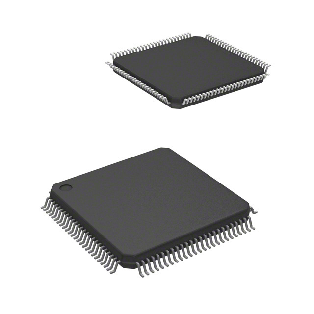
- Package: 100-pin plastic quad flat pack (PQFP)
- Essence: Provides fast and reliable data storage and retrieval capabilities
- Packaging/Quantity: Available in tape and reel packaging, quantity varies based on customer requirements
Specifications
- Memory Type: Synchronous SRAM
- Memory Size: 256K x 36 bits
- Operating Voltage: 3.3V
- Access Time: 10 ns
- Operating Temperature Range: -40°C to +85°C
- Data Retention: Greater than 10 years
- Interface: Parallel
- Clock Frequency: 100 MHz
- Power Consumption: Low power consumption design
Pin Configuration
The IDT71V2546S100PFI8 has a total of 100 pins. The pin configuration is as follows:
- VDDQ
- DQ0
- DQ1
- DQ2
- DQ3
- DQ4
- DQ5
- DQ6
- DQ7
- DQ8
- DQ9
- DQ10
- DQ11
- DQ12
- DQ13
- DQ14
- DQ15
- DQ16
- DQ17
- DQ18
- DQ19
- DQ20
- DQ21
- DQ22
- DQ23
- DQ24
- DQ25
- DQ26
- DQ27
- DQ28
- DQ29
- DQ30
- DQ31
- VSSQ
- A0
- A1
- A2
- A3
- A4
- A5
- A6
- A7
- A8
- A9
- A10
- A11
- A12
- A13
- A14
- A15
- A16
- A17
- A18
- A19
- A20
- A21
- A22
- A23
- A24
- A25
- A26
- A27
- A28
- A29
- A30
- A31
- CE#
- WE#
- OE#
- UB#
- LB#
- CLK
- CLKEN#
- CKE#
- CS#
- RAS#
- CAS#
- WEN#
- OEN#
- BHE#
- BLE#
- BYTE#
- ADSP#
- ADSC#
- ADSP#
- ADSC#
- ADSP#
- ADSC#
- ADSP#
- ADSC#
- ADSP#
- ADSC#
- ADSP#
- ADSC#
- ADSP#
- ADSC#
- ADSP#
- ADSC#
- ADSP#
- ADSC#
Functional Features
- High-speed operation allows for quick data access and retrieval
- Low-power design reduces energy consumption
- Synchronous interface ensures reliable data transfer
- Wide operating temperature range enables usage in various environments
- Large memory size provides ample storage capacity
Advantages and Disadvantages
Advantages: - Fast access time and high-speed operation - Low power consumption - Reliable synchronous interface - Ample storage capacity
Disadvantages: - Limited compatibility with certain systems due to specific pin configuration - Relatively higher cost compared to other memory devices
Working Principles
The IDT71V2546S100PFI8 is a synchronous SRAM that operates based on the synchronous interface. It uses an internal clock signal (CLK) to synchronize data transfers between the memory device and the connected system. The device supports read and write operations, allowing for efficient data storage and retrieval.
Detailed Application Field Plans
The IDT71V2546S100PFI8 can be used in various applications that require high-speed and reliable data storage. Some potential application fields include:
- Networking equipment
- Telecommunications systems
- Industrial automation
- Medical
Lista 10 Vanliga frågor och svar relaterade till tillämpningen av IDT71V2546S100PFI8 i tekniska lösningar
Sure! Here are 10 common questions and answers related to the application of IDT71V2546S100PFI8 in technical solutions:
Question: What is the IDT71V2546S100PFI8?
Answer: The IDT71V2546S100PFI8 is a high-speed, low-power CMOS static RAM (SRAM) with a capacity of 256K (32K x 8) bits.Question: What are the key features of the IDT71V2546S100PFI8?
Answer: Some key features include a fast access time of 10ns, low power consumption, wide operating voltage range, and a small form factor.Question: What are some typical applications for the IDT71V2546S100PFI8?
Answer: This SRAM can be used in various applications such as networking equipment, telecommunications systems, industrial automation, and embedded systems.Question: What is the operating voltage range for the IDT71V2546S100PFI8?
Answer: The IDT71V2546S100PFI8 operates within a voltage range of 3.0V to 3.6V.Question: Can the IDT71V2546S100PFI8 be used in battery-powered devices?
Answer: Yes, the low power consumption of this SRAM makes it suitable for use in battery-powered devices where power efficiency is crucial.Question: Does the IDT71V2546S100PFI8 support multiple read and write operations simultaneously?
Answer: No, this SRAM does not support simultaneous multiple read or write operations.Question: What is the package type for the IDT71V2546S100PFI8?
Answer: The IDT71V2546S100PFI8 is available in a 32-pin plastic leaded chip carrier (PLCC) package.Question: What is the maximum operating frequency of the IDT71V2546S100PFI8?
Answer: The maximum operating frequency for this SRAM is 100MHz.Question: Can the IDT71V2546S100PFI8 operate in harsh environmental conditions?
Answer: Yes, this SRAM is designed to operate within a wide temperature range (-40°C to +85°C) and can withstand harsh environmental conditions.Question: Is the IDT71V2546S100PFI8 pin-compatible with other SRAMs?
Answer: No, it is important to verify pin compatibility with other SRAMs before replacing them with the IDT71V2546S100PFI8.
Please note that these answers are general and may vary depending on specific technical requirements and application scenarios.