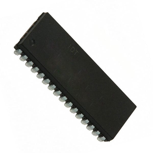
IDT71V124SA20TYI8
Product Overview
Category
The IDT71V124SA20TYI8 belongs to the category of Static Random Access Memory (SRAM).
Use
This product is primarily used as a high-speed, low-power memory solution in various electronic devices and systems.
Characteristics
- High-speed operation: The IDT71V124SA20TYI8 offers fast access times, making it suitable for applications that require quick data retrieval.
- Low power consumption: This SRAM module is designed to minimize power consumption, making it ideal for battery-powered devices.
- Large storage capacity: With a capacity of 1 Megabit (128K x 8), this SRAM chip can store a significant amount of data.
- Reliable performance: The IDT71V124SA20TYI8 ensures reliable data storage and retrieval, providing stable operation over extended periods.
Package
The IDT71V124SA20TYI8 is available in a compact Thin Small Outline Package (TSOP) format. This package offers a small footprint, making it suitable for space-constrained applications.
Essence
The essence of the IDT71V124SA20TYI8 lies in its ability to provide high-speed, low-power memory storage, enabling efficient data processing in electronic devices.
Packaging/Quantity
This product is typically packaged in reels or trays, with each reel or tray containing a specific quantity of IDT71V124SA20TYI8 chips. The exact quantity may vary depending on the manufacturer's specifications.
Specifications
- Organization: 128K x 8 bits
- Operating Voltage: 3.3V
- Access Time: 20 ns
- Standby Current: 10 µA (typical)
- Operating Temperature Range: -40°C to +85°C
- Data Retention: 10 years (minimum)
Detailed Pin Configuration
The IDT71V124SA20TYI8 has a total of 32 pins, which are assigned specific functions. The pin configuration is as follows:
- Chip Enable (CE)
- Output Enable (OE)
- Write Enable (WE)
- Address Inputs (A0-A16)
- Data Inputs/Outputs (DQ0-DQ7)
- Power Supply (VCC)
- Ground (GND)
Please refer to the datasheet for a complete pinout diagram and detailed pin descriptions.
Functional Features
- Asynchronous operation: The IDT71V124SA20TYI8 does not require a clock signal for data access, allowing for flexible integration into various systems.
- Byte-wide access: This SRAM chip supports byte-wide access, enabling efficient data manipulation and transfer.
- Easy interfacing: The IDT71V124SA20TYI8 can be easily connected to microcontrollers or other devices using standard digital interface protocols.
Advantages and Disadvantages
Advantages
- High-speed operation allows for quick data access and processing.
- Low power consumption prolongs battery life in portable devices.
- Large storage capacity accommodates significant amounts of data.
- Reliable performance ensures stable operation over extended periods.
Disadvantages
- Limited storage capacity compared to other memory technologies like NAND Flash or Hard Disk Drives.
- Volatile memory requires continuous power supply to retain data.
Working Principles
The IDT71V124SA20TYI8 operates based on the principles of static random access memory. It stores data in a matrix of flip-flops, where each flip-flop represents a single bit of information. The stored data can be accessed by providing the appropriate address and control signals.
When a read operation is initiated, the addressed data is retrieved from the memory array and made available on the data output pins. Similarly, during a write operation, the data to be stored is provided to the input pins and written into the corresponding memory location.
Detailed Application Field Plans
The IDT71V124SA20TYI8 finds applications in various electronic systems that require high-speed, low-power memory solutions. Some potential application fields include:
- Embedded Systems: The SRAM module can be used in embedded systems such as microcontrollers, where fast data access is crucial for efficient operation.
- Networking Equipment: The IDT71V124SA20TYI8 can be employed in routers, switches, and other networking devices to store routing tables and temporary data.
- Industrial Automation: This SRAM chip can be utilized in industrial automation systems for storing real-time data, configuration settings, and program code.
- Medical Devices: The IDT71V124SA20TYI8 can be integrated into medical devices like patient monitors or diagnostic equipment, where quick data retrieval is essential.
Detailed and Complete Alternative Models
- IDT71V124SA15TYI8: Similar to the IDT71V124SA
Lista 10 Vanliga frågor och svar relaterade till tillämpningen av IDT71V124SA20TYI8 i tekniska lösningar
Sure! Here are 10 common questions and answers related to the application of IDT71V124SA20TYI8 in technical solutions:
Q: What is the IDT71V124SA20TYI8? A: The IDT71V124SA20TYI8 is a high-speed, low-power CMOS static RAM (SRAM) with a capacity of 128K x 8 bits.
Q: What are the typical applications of IDT71V124SA20TYI8? A: This SRAM can be used in various applications such as networking equipment, telecommunications systems, industrial automation, and embedded systems.
Q: What is the operating voltage range for IDT71V124SA20TYI8? A: The operating voltage range for this SRAM is typically between 4.5V and 5.5V.
Q: What is the access time of IDT71V124SA20TYI8? A: The access time of this SRAM is 20ns, which means it takes 20 nanoseconds to read or write data.
Q: Does IDT71V124SA20TYI8 support multiple chip enable inputs? A: Yes, this SRAM supports two chip enable inputs (CE1 and CE2), allowing for easy interfacing with other devices.
Q: Can I use IDT71V124SA20TYI8 in battery-powered devices? A: Yes, this SRAM has low power consumption, making it suitable for battery-powered devices where power efficiency is crucial.
Q: What is the standby current of IDT71V124SA20TYI8? A: The standby current of this SRAM is typically less than 10µA, ensuring minimal power consumption when not actively accessing data.
Q: Does IDT71V124SA20TYI8 have any built-in error correction capabilities? A: No, this SRAM does not have built-in error correction capabilities. Additional error correction techniques may be required for critical applications.
Q: Can I use IDT71V124SA20TYI8 in high-temperature environments? A: Yes, this SRAM is designed to operate reliably in a wide temperature range, typically from -40°C to 85°C.
Q: Is IDT71V124SA20TYI8 available in different package options? A: Yes, this SRAM is available in various package options, including 32-pin TSOP and 32-pin TQFP, providing flexibility for different system designs.
Please note that the answers provided here are general and may vary depending on the specific datasheet and manufacturer's specifications for the IDT71V124SA20TYI8 SRAM.


