

IDT5V9885BPFI
Product Overview
- Category: Integrated Circuit (IC)
- Use: Voltage Level Translator
- Characteristics: High-speed, bidirectional voltage translation between different logic levels
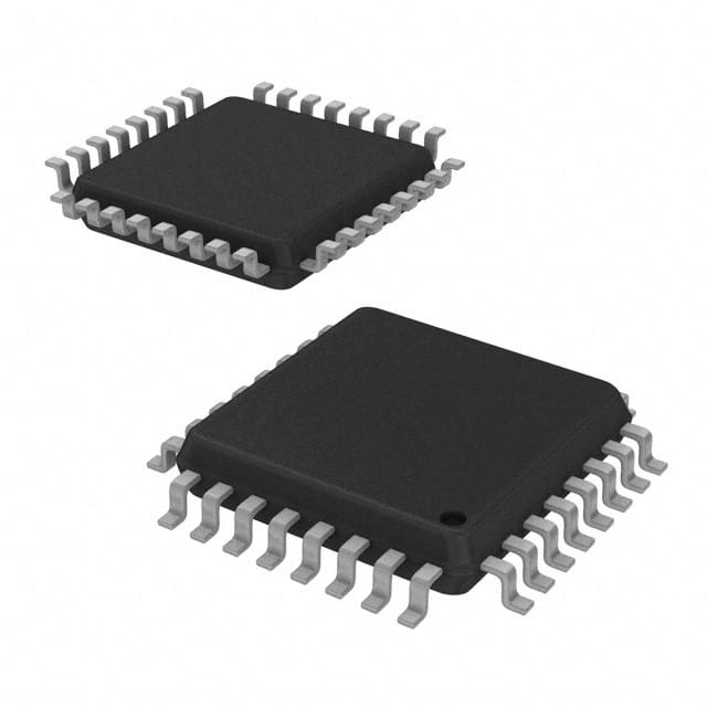
- Package: 48-pin TQFP (Thin Quad Flat Package)
- Essence: Efficiently translates voltage levels to enable communication between devices operating at different logic levels
- Packaging/Quantity: Available in tape and reel packaging, with a quantity of 250 units per reel
Specifications
- Supply Voltage: 1.2V - 3.6V
- Logic Voltage Levels Supported: 1.2V, 1.8V, 2.5V, 3.3V
- Data Rate: Up to 100 Mbps
- Number of Channels: 8
- Operating Temperature Range: -40°C to +85°C
Detailed Pin Configuration
The IDT5V9885BPFI features a 48-pin TQFP package with the following pin configuration:
- VCCA - Supply voltage for side A
- GND - Ground
- A1 - Channel A1 input/output
- B1 - Channel B1 input/output
- A2 - Channel A2 input/output
- B2 - Channel B2 input/output
- A3 - Channel A3 input/output
- B3 - Channel B3 input/output
- A4 - Channel A4 input/output
- B4 - Channel B4 input/output
- A5 - Channel A5 input/output
- B5 - Channel B5 input/output
- A6 - Channel A6 input/output
- B6 - Channel B6 input/output
- A7 - Channel A7 input/output
- B7 - Channel B7 input/output
- A8 - Channel A8 input/output
- B8 - Channel B8 input/output
- VCCB - Supply voltage for side B
- OE - Output enable
- GND - Ground
- VREF - Reference voltage
- GND - Ground
- VCCA - Supply voltage for side A
- GND - Ground
- VCCB - Supply voltage for side B
Functional Features
- Bidirectional voltage translation between different logic levels
- Automatic direction sensing and control
- Low power consumption
- High-speed data transmission
- ESD (Electrostatic Discharge) protection on all pins
- Supports multiple logic voltage levels
Advantages and Disadvantages
Advantages: - Efficient voltage level translation for seamless communication between devices - Automatic direction sensing simplifies system design - High-speed data transmission enables fast communication - ESD protection ensures reliability in harsh environments
Disadvantages: - Limited to 8 channels, may not be suitable for applications requiring a higher number of channels - Requires careful consideration of power supply voltages to ensure proper operation
Working Principles
The IDT5V9885BPFI operates by receiving input signals from one logic level and translating them to the corresponding logic level on the other side. It automatically senses the direction of the data flow and adjusts the voltage translation accordingly. The device utilizes internal circuitry to achieve bidirectional voltage translation while maintaining high-speed data transmission and low power consumption.
Detailed Application Field Plans
The IDT5V9885BPFI is widely used in various applications that require voltage level translation between different logic levels. Some common application fields include:
- Microcontroller interfacing with different peripheral devices
- Communication interfaces between different integrated circuits
- Signal conversion between different logic
Lista 10 Vanliga frågor och svar relaterade till tillämpningen av IDT5V9885BPFI i tekniska lösningar
Sure! Here are 10 common questions and answers related to the application of IDT5V9885BPFI in technical solutions:
Question: What is IDT5V9885BPFI?
Answer: IDT5V9885BPFI is a high-performance clock generator and fanout buffer designed for use in various technical solutions.Question: What is the purpose of IDT5V9885BPFI?
Answer: The purpose of IDT5V9885BPFI is to generate and distribute stable clock signals to multiple components within a system.Question: What are the key features of IDT5V9885BPFI?
Answer: Some key features of IDT5V9885BPFI include low phase noise, low skew, multiple outputs, and programmable output frequencies.Question: In which applications can IDT5V9885BPFI be used?
Answer: IDT5V9885BPFI can be used in a wide range of applications such as data centers, telecommunications, networking equipment, and high-speed digital systems.Question: How many outputs does IDT5V9885BPFI support?
Answer: IDT5V9885BPFI supports up to 12 differential outputs, making it suitable for driving multiple devices simultaneously.Question: Can the output frequencies of IDT5V9885BPFI be programmed?
Answer: Yes, the output frequencies of IDT5V9885BPFI can be programmed using an external I2C interface or by configuring the device pins.Question: Does IDT5V9885BPFI support different voltage levels?
Answer: Yes, IDT5V9885BPFI supports both LVCMOS and LVDS voltage levels, providing flexibility in connecting to various components.Question: What is the power supply voltage range for IDT5V9885BPFI?
Answer: The power supply voltage range for IDT5V9885BPFI is typically between 3.135V and 3.465V.Question: Can IDT5V9885BPFI be used in high-speed data transmission applications?
Answer: Yes, IDT5V9885BPFI is designed to support high-speed data transmission with low jitter and skew characteristics.Question: Are there any evaluation boards or reference designs available for IDT5V9885BPFI?
Answer: Yes, IDT provides evaluation boards and reference designs that can help users quickly integrate IDT5V9885BPFI into their technical solutions.
Please note that these answers are general and may vary depending on specific requirements and use cases.