

IDT5V9885BPFGI8
Product Overview
- Category: Integrated Circuit (IC)
- Use: Signal Switching and Timing Solution
- Characteristics: High-performance, low-power, compact design
- Package: BGA (Ball Grid Array)
- Essence: Advanced signal switching and timing capabilities
- Packaging/Quantity: Available in tape and reel packaging, quantity varies based on customer requirements
Specifications
- Manufacturer: Integrated Device Technology (IDT)
- Part Number: IDT5V9885BPFGI8
- Technology: CMOS (Complementary Metal-Oxide-Semiconductor)
- Operating Voltage: 1.8V - 3.3V
- Operating Temperature: -40°C to +85°C
- Number of Channels: 8
- Switching Frequency: Up to 200 MHz
- Input/Output Type: LVCMOS (Low-Voltage Complementary Metal-Oxide-Semiconductor)
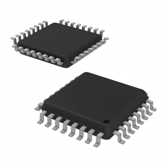
- Package Type: 56-ball VFBGA (Very Fine Pitch Ball Grid Array)
- Dimensions: 4mm x 4mm
Detailed Pin Configuration
The IDT5V9885BPFGI8 features a 56-ball VFBGA package with the following pin configuration:
- GND
- IN1
- OUT1
- IN2
- OUT2
- IN3
- OUT3
- IN4
- OUT4
- IN5
- OUT5
- IN6
- OUT6
- IN7
- OUT7
- IN8
- OUT8
- GND
- OE#
- VDD
- GND
- GND
- GND
- GND
- GND
- GND
- GND
- GND
- GND
- GND
- GND
- GND
- GND
- GND
- GND
- GND
- GND
- GND
- GND
- GND
- GND
- GND
- GND
- GND
- GND
- GND
- GND
- GND
- GND
- GND
- GND
- GND
- GND
- GND
- GND
- GND
Functional Features
- High-speed signal switching capability
- Low power consumption
- Wide operating voltage range
- Excellent signal integrity and reliability
- Integrated ESD (Electrostatic Discharge) protection
- Flexible control options with OE# pin
Advantages and Disadvantages
Advantages
- High-performance signal switching solution
- Compact design suitable for space-constrained applications
- Low power consumption extends battery life
- Robust ESD protection ensures device reliability
- Versatile control options enhance system flexibility
Disadvantages
- Limited number of channels (8)
- Relatively high cost compared to simpler alternatives
Working Principles
The IDT5V9885BPFGI8 is designed to provide efficient signal switching and timing capabilities in various electronic systems. It utilizes CMOS technology, allowing for high-speed operation while maintaining low power consumption. The device features 8 channels, each capable of handling LVCMOS signals. The integrated ESD protection safeguards the IC from electrostatic discharge events, ensuring reliable performance.
The IDT5V9885BPFGI8 can be controlled using the OE# (Output Enable) pin, which allows for easy system integration and flexibility. When the OE# pin is low, the outputs are enabled, allowing signals to pass through. Conversely, when the OE# pin is high, the outputs are disabled, effectively isolating the input signals.
Detailed Application Field Plans
The IDT5V9885BPFGI8 finds applications in various fields, including:
- Communication Systems: Used for signal routing and switching in telecommunication equipment, routers, and switches.
- Test and Measurement Instruments: Enables signal multiplexing and switching in oscilloscopes, logic analyzers, and data acquisition systems.
- Industrial Automation: Facilitates signal routing and timing synchronization in programmable logic controllers (PLCs), motor control systems, and industrial sensors.
- Consumer Electronics: Utilized in audio/video equipment, gaming consoles, and home automation systems for signal routing and synchronization.
- Automotive Electronics: Enables signal switching and timing in automotive infotainment systems, instrument clusters, and advanced driver-assistance systems (AD
Lista 10 Vanliga frågor och svar relaterade till tillämpningen av IDT5V9885BPFGI8 i tekniska lösningar
Sure! Here are 10 common questions and answers related to the application of IDT5V9885BPFGI8 in technical solutions:
Q: What is the IDT5V9885BPFGI8? A: The IDT5V9885BPFGI8 is a high-performance clock generator and fanout buffer designed for use in various technical solutions.
Q: What are the key features of the IDT5V9885BPFGI8? A: The key features include low phase noise, multiple outputs, programmable output frequencies, and support for various input reference frequencies.
Q: What is the purpose of using the IDT5V9885BPFGI8 in technical solutions? A: The IDT5V9885BPFGI8 is used to generate and distribute precise clock signals to different components within a system, ensuring synchronization and proper timing.
Q: How many outputs does the IDT5V9885BPFGI8 have? A: The IDT5V9885BPFGI8 has up to 12 differential clock outputs, providing flexibility in distributing clock signals to multiple devices.
Q: Can the output frequencies be programmed on the IDT5V9885BPFGI8? A: Yes, the IDT5V9885BPFGI8 supports programmable output frequencies, allowing customization based on specific system requirements.
Q: What is the typical phase noise performance of the IDT5V9885BPFGI8? A: The IDT5V9885BPFGI8 offers low phase noise performance, typically below -150 dBc/Hz at 100 kHz offset.
Q: What input reference frequencies does the IDT5V9885BPFGI8 support? A: The IDT5V9885BPFGI8 supports input reference frequencies ranging from 10 MHz to 700 MHz.
Q: Can the IDT5V9885BPFGI8 be used in high-speed data communication applications? A: Yes, the IDT5V9885BPFGI8 is suitable for high-speed data communication applications, providing reliable clock distribution and synchronization.
Q: Does the IDT5V9885BPFGI8 require external programming or configuration? A: No, the IDT5V9885BPFGI8 has an integrated EEPROM that stores default settings, eliminating the need for external programming.
Q: What is the operating voltage range of the IDT5V9885BPFGI8? A: The IDT5V9885BPFGI8 operates within a voltage range of 2.375V to 3.63V, making it compatible with various power supply systems.
Please note that these questions and answers are general and may vary depending on specific application requirements.