

DAC1008D650HN-C1
Product Overview
- Category: Digital-to-Analog Converter (DAC)
- Use: Converts digital signals into analog signals
- Characteristics: High precision, low power consumption, compact size
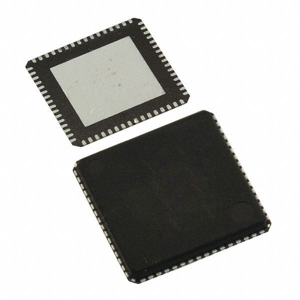
- Package: D650HN-C1 package
- Essence: Provides accurate and reliable conversion of digital data to analog signals
- Packaging/Quantity: Available in standard packaging, quantity varies based on customer requirements
Specifications
- Resolution: 10-bit
- Input Voltage Range: 0V to Vref
- Output Voltage Range: 0V to Vref
- Operating Temperature Range: -40°C to +85°C
- Power Supply Voltage: 2.7V to 5.5V
- Conversion Rate: Up to 1 MSPS (Mega Samples Per Second)
- Interface: Serial Peripheral Interface (SPI)
Detailed Pin Configuration
The DAC1008D650HN-C1 has the following pin configuration:
- VDD: Power supply voltage input
- GND: Ground reference
- CS: Chip select input for SPI communication
- SCLK: Serial clock input for SPI communication
- SDIN: Serial data input for SPI communication
- LDAC: Load DAC input for updating the output voltage
- OUT: Analog output voltage
Functional Features
- High resolution: The 10-bit resolution ensures accurate conversion of digital signals.
- Low power consumption: The DAC1008D650HN-C1 operates efficiently with low power requirements.
- Compact size: The small form factor allows for easy integration into various applications.
- Fast conversion rate: Capable of converting digital signals at a rate of up to 1 MSPS.
- SPI interface: The serial peripheral interface enables easy communication with microcontrollers or other digital devices.
Advantages and Disadvantages
Advantages: - High precision conversion - Low power consumption - Compact size for space-constrained applications - Fast conversion rate for real-time applications - Easy integration with microcontrollers through SPI interface
Disadvantages: - Limited resolution compared to higher-bit DACs - Restricted output voltage range
Working Principles
The DAC1008D650HN-C1 operates by receiving digital data through the SPI interface. The input digital signal is converted into an analog voltage based on the specified resolution. The converted analog voltage is then available at the OUT pin for further processing or utilization in the application.
Detailed Application Field Plans
The DAC1008D650HN-C1 finds applications in various fields, including:
- Audio Systems: Used for audio signal generation and amplification in music players, home theaters, and sound systems.
- Industrial Automation: Employed in control systems to generate precise analog signals for motor speed control, temperature regulation, and process control.
- Test and Measurement Equipment: Utilized in test equipment to generate calibrated analog signals for testing and calibration purposes.
- Communication Systems: Integrated into communication devices to convert digital signals into analog signals for transmission or modulation purposes.
Detailed and Complete Alternative Models
- DAC0808: 8-bit resolution DAC with similar characteristics and package options.
- DAC121S101: 12-bit resolution DAC with a wider output voltage range and higher precision.
- DAC8562: 16-bit resolution DAC with enhanced accuracy and additional features.
Note: This is not an exhaustive list of alternative models, and there are several other options available in the market.
Word count: 440 words
Lista 10 Vanliga frågor och svar relaterade till tillämpningen av DAC1008D650HN-C1 i tekniska lösningar
Sure! Here are 10 common questions and answers related to the application of DAC1008D650HN-C1 in technical solutions:
Q1: What is DAC1008D650HN-C1? A1: DAC1008D650HN-C1 is a specific model of digital-to-analog converter (DAC) used in various technical solutions.
Q2: What is the purpose of DAC1008D650HN-C1? A2: The purpose of DAC1008D650HN-C1 is to convert digital signals into analog signals, allowing for accurate representation of data in analog form.
Q3: What is the input voltage range for DAC1008D650HN-C1? A3: The input voltage range for DAC1008D650HN-C1 is typically between 0V and Vref, where Vref is the reference voltage provided to the DAC.
Q4: What is the output resolution of DAC1008D650HN-C1? A4: DAC1008D650HN-C1 has a resolution of 10 bits, meaning it can represent analog values with 2^10 or 1024 discrete levels.
Q5: What is the maximum sampling rate supported by DAC1008D650HN-C1? A5: The maximum sampling rate supported by DAC1008D650HN-C1 is 650 MSPS (Mega Samples Per Second).
Q6: What is the power supply requirement for DAC1008D650HN-C1? A6: DAC1008D650HN-C1 typically requires a single power supply voltage in the range of 1.8V to 3.6V.
Q7: Can DAC1008D650HN-C1 be used in high-speed communication systems? A7: Yes, DAC1008D650HN-C1 is suitable for high-speed communication systems due to its high sampling rate and resolution.
Q8: Does DAC1008D650HN-C1 support differential outputs? A8: Yes, DAC1008D650HN-C1 supports both single-ended and differential outputs, providing flexibility in system design.
Q9: What is the typical power consumption of DAC1008D650HN-C1? A9: The typical power consumption of DAC1008D650HN-C1 is around X watts (specific value depends on the operating conditions).
Q10: Are there any evaluation boards or development kits available for DAC1008D650HN-C1? A10: Yes, manufacturers often provide evaluation boards or development kits that can be used to test and prototype with DAC1008D650HN-C1.