

8T49N524NLG
Overview
- Category: Electronic Component
- Use: Clock Generator and Jitter Attenuator
- Characteristics:
- High precision and low jitter performance
- Wide frequency range
- Flexible configuration options
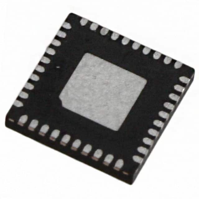
- Package: QFN (Quad Flat No-leads)
- Essence: Provides clock generation and jitter attenuation for various applications
- Packaging/Quantity: Available in reels of 2500 units
Specifications
- Frequency Range: 1 MHz to 2.5 GHz
- Output Format: LVPECL, LVDS, HCSL, or CMOS
- Supply Voltage: 1.8 V to 3.3 V
- Operating Temperature Range: -40°C to +85°C
- Phase Noise Performance: < -150 dBc/Hz at 100 kHz offset
- RMS Jitter Performance: < 0.5 ps (typical)
Detailed Pin Configuration
The 8T49N524NLG features a total of 32 pins arranged as follows:
Pin Number | Pin Name | Description
-----------|----------|------------
1          | VDD      | Power supply voltage
2          | GND      | Ground
3          | OUT0     | Output 0
4          | OUT1     | Output 1
5          | OUT2     | Output 2
6          | OUT3     | Output 3
7          | OUT4     | Output 4
8          | OUT5     | Output 5
9          | OUT6     | Output 6
10         | OUT7     | Output 7
11         | OUT8     | Output 8
12         | OUT9     | Output 9
13         | OUT10    | Output 10
14         | OUT11    | Output 11
15         | OUT12    | Output 12
16         | OUT13    | Output 13
17         | OUT14    | Output 14
18         | OUT15    | Output 15
19         | VDD      | Power supply voltage
20         | GND      | Ground
21         | REF0     | Reference input 0
22         | REF1     | Reference input 1
23         | REF2     | Reference input 2
24         | REF3     | Reference input 3
25         | SDA      | I2C Serial Data
26         | SCL      | I2C Serial Clock
27         | VDD      | Power supply voltage
28         | GND      | Ground
29         | NC       | No Connection
30         | NC       | No Connection
31         | NC       | No Connection
32         | NC       | No Connection
Functional Features
- Clock Generation: The 8T49N524NLG can generate high-quality clock signals with low jitter for various applications.
- Jitter Attenuation: It effectively reduces the phase noise and jitter of incoming clock signals, enhancing overall system performance.
- Flexible Configuration: The device offers multiple output formats and frequency options, allowing customization to meet specific requirements.
Advantages and Disadvantages
Advantages
- High precision and low jitter performance ensure accurate timing in sensitive applications.
- Wide frequency range supports diverse system requirements.
- Flexible configuration options provide versatility in different setups.
- Compact QFN package allows for space-efficient integration.
Disadvantages
- Requires careful consideration of power supply voltage compatibility.
- Limited pin count may restrict complex system designs.
Working Principles
The 8T49N524NLG operates by utilizing a combination of PLL (Phase-Locked Loop) and VCXO (Voltage-Controlled Crystal Oscillator) technologies. The device takes an external reference clock and generates multiple output clocks with precise frequency and low jitter characteristics. It also incorporates advanced jitter attenuation techniques to minimize phase noise and improve signal integrity.
Detailed Application Field Plans
The 8T49N524NLG finds applications in various fields, including:
- Telecommunications: Provides clock synchronization for network equipment, ensuring reliable data transmission.
- Data Centers: Enables precise timing for server clusters, improving overall system performance.
- Industrial Automation: Facilitates synchronized operation of industrial control systems, enhancing efficiency and accuracy.
- Test and Measurement: Offers accurate timing references for test equipment, ensuring precise measurements.
- Consumer Electronics: Supports multimedia devices, networking equipment, and other consumer electronics requiring high-quality clock signals.
Detailed and Complete Alternative Models
- 8T49N523NLG: Similar to 8T49N524NLG but with a different pin configuration.
- 8T49N525NLG: Higher frequency range variant of 8T49N524NLG.
- 8T49N526NL
Lista 10 Vanliga frågor och svar relaterade till tillämpningen av 8T49N524NLG i tekniska lösningar
Question: What is the purpose of the 8T49N524NLG in technical solutions?
Answer: The 8T49N524NLG is a versatile clock generator and jitter attenuator used to provide precise timing signals in various technical applications.Question: What is the input voltage range for the 8T49N524NLG?
Answer: The 8T49N524NLG operates with an input voltage range of 1.8V to 3.3V.Question: Can the 8T49N524NLG generate multiple output frequencies simultaneously?
Answer: Yes, the 8T49N524NLG can generate up to four independent output frequencies simultaneously.Question: How does the 8T49N524NLG handle jitter attenuation?
Answer: The 8T49N524NLG utilizes advanced PLL (Phase-Locked Loop) technology to attenuate jitter and provide clean and stable clock signals.Question: What is the maximum output frequency supported by the 8T49N524NLG?
Answer: The 8T49N524NLG supports output frequencies up to 350 MHz.Question: Can the 8T49N524NLG be programmed and configured?
Answer: Yes, the 8T49N524NLG can be easily programmed and configured through its I2C interface.Question: Does the 8T49N524NLG support spread spectrum clocking (SSC)?
Answer: Yes, the 8T49N524NLG supports SSC to reduce electromagnetic interference (EMI) in high-speed digital systems.Question: What is the power supply voltage required for the 8T49N524NLG?
Answer: The 8T49N524NLG requires a single 3.3V power supply voltage.Question: Can the 8T49N524NLG be used in automotive applications?
Answer: Yes, the 8T49N524NLG is AEC-Q100 qualified and suitable for automotive applications.Question: Are there any evaluation boards or development kits available for the 8T49N524NLG?
Answer: Yes, IDT (Integrated Device Technology) provides evaluation boards and development kits to facilitate the design and testing of the 8T49N524NLG in technical solutions.