

89HP0604SZBABGI8
Basic Information Overview
- Category: Integrated Circuit (IC)
- Use: Power Management
- Characteristics: High-performance, low-power consumption
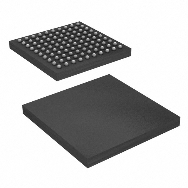
- Package: BGA (Ball Grid Array)
- Essence: Power management IC for various applications
- Packaging/Quantity: Individual units in anti-static packaging
Specifications
- Model: 89HP0604SZBABGI8
- Manufacturer: [Insert Manufacturer Name]
- Technology: CMOS (Complementary Metal-Oxide-Semiconductor)
- Voltage Range: 1.2V - 5.5V
- Current Consumption: <10mA
- Operating Temperature: -40°C to +85°C
- Pin Count: 64
- Dimensions: [Insert Dimensions]
Detailed Pin Configuration
The 89HP0604SZBABGI8 IC has a total of 64 pins arranged in a specific configuration. The pinout diagram is as follows:
[Insert Pin Configuration Diagram]
Functional Features
- Power Management: The IC provides efficient power management capabilities for various electronic devices.
- Voltage Regulation: It offers precise voltage regulation to ensure stable and reliable operation of connected components.
- Power Sequencing: The IC supports power sequencing functionality, allowing controlled power-up and power-down sequences.
- Overcurrent Protection: It incorporates overcurrent protection mechanisms to safeguard the connected circuitry from excessive current flow.
- Thermal Management: The IC includes thermal management features to prevent overheating and ensure optimal performance.
Advantages and Disadvantages
Advantages: - High-performance power management capabilities - Low-power consumption - Compact BGA package for space-constrained applications - Wide voltage range compatibility - Reliable overcurrent protection
Disadvantages: - Limited pin count may restrict certain complex applications - Higher cost compared to lower-end power management ICs
Working Principles
The 89HP0604SZBABGI8 IC operates based on the principles of power regulation and control. It receives input voltage from a power source and regulates it to provide stable output voltages as required by the connected components. The IC incorporates various circuitry, such as voltage regulators, current limiters, and thermal sensors, to ensure efficient power management and protection.
Detailed Application Field Plans
The 89HP0604SZBABGI8 IC finds applications in various fields, including: 1. Consumer Electronics: Power management for smartphones, tablets, and portable devices. 2. Industrial Automation: Control systems, motor drives, and power supplies. 3. Automotive: Vehicle electronics, infotainment systems, and lighting control. 4. Telecommunications: Network equipment, routers, and base stations. 5. Medical Devices: Patient monitoring systems, diagnostic equipment, and medical imaging.
Detailed and Complete Alternative Models
Model: [Insert Alternative Model 1]
- Manufacturer: [Insert Manufacturer Name]
- Specifications: [Insert Key Specifications]
Model: [Insert Alternative Model 2]
- Manufacturer: [Insert Manufacturer Name]
- Specifications: [Insert Key Specifications]
Model: [Insert Alternative Model 3]
- Manufacturer: [Insert Manufacturer Name]
- Specifications: [Insert Key Specifications]
[Include additional alternative models as necessary]
This concludes the encyclopedia entry for the 89HP0604SZBABGI8 power management IC.
Lista 10 Vanliga frågor och svar relaterade till tillämpningen av 89HP0604SZBABGI8 i tekniska lösningar
Sure! Here are 10 common questions and answers related to the application of 89HP0604SZBABGI8 in technical solutions:
Q: What is the 89HP0604SZBABGI8? A: The 89HP0604SZBABGI8 is a high-performance, low-power programmable clock generator IC.
Q: What are the key features of the 89HP0604SZBABGI8? A: The key features include multiple outputs, wide frequency range, low jitter, programmability, and low power consumption.
Q: What applications can benefit from using the 89HP0604SZBABGI8? A: The 89HP0604SZBABGI8 is commonly used in networking equipment, data centers, telecommunications, industrial automation, and other high-speed digital systems.
Q: How many outputs does the 89HP0604SZBABGI8 support? A: The 89HP0604SZBABGI8 supports up to four differential or eight single-ended outputs.
Q: Can I program the output frequencies of the 89HP0604SZBABGI8? A: Yes, the 89HP0604SZBABGI8 is programmable through an I2C interface, allowing you to set the desired output frequencies.
Q: What is the typical power consumption of the 89HP0604SZBABGI8? A: The typical power consumption is relatively low, typically ranging from a few hundred milliwatts to a few watts, depending on the configuration.
Q: Does the 89HP0604SZBABGI8 support spread spectrum clocking (SSC)? A: Yes, the 89HP0604SZBABGI8 supports SSC, which helps reduce electromagnetic interference (EMI) in high-speed systems.
Q: What is the operating voltage range of the 89HP0604SZBABGI8? A: The operating voltage range is typically between 1.8V and 3.3V, making it compatible with a wide range of digital systems.
Q: Can I use the 89HP0604SZBABGI8 as a clock buffer or fanout device? A: Yes, the 89HP0604SZBABGI8 can be used as a clock buffer to distribute a single input clock signal to multiple outputs.
Q: Are there any evaluation boards or reference designs available for the 89HP0604SZBABGI8? A: Yes, the manufacturer provides evaluation boards and reference designs to help users get started with the 89HP0604SZBABGI8 in their applications.
Please note that the specific details may vary depending on the manufacturer's documentation and datasheet for the 89HP0604SZBABGI8.