

Encyclopedia Entry: 89HP0504PZBNRG8
Product Information Overview
Category: Integrated Circuit (IC)
Use: The 89HP0504PZBNRG8 is a high-performance programmable logic device designed for use in various electronic systems. It offers advanced functionality and flexibility, making it suitable for a wide range of applications.
Characteristics: This IC features a high-speed interface, low power consumption, and excellent signal integrity. It is known for its reliability and robustness, ensuring optimal performance even in demanding environments.
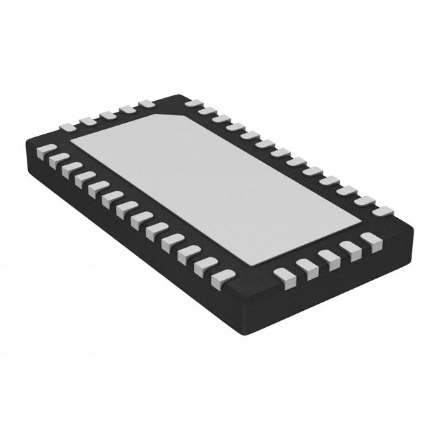
Package: The 89HP0504PZBNRG8 comes in a compact and durable package, which protects the integrated circuit from external factors such as moisture and physical damage. The package also facilitates easy installation and integration into electronic systems.
Essence: The essence of the 89HP0504PZBNRG8 lies in its ability to provide efficient and reliable programmable logic capabilities, enabling designers to implement complex functions and algorithms in their electronic systems.
Packaging/Quantity: Each package contains one 89HP0504PZBNRG8 integrated circuit.
Specifications
- Logic Family: High-Performance CPLD
- Number of Macrocells: 504
- Operating Voltage: 3.3V
- Maximum Frequency: 200MHz
- I/O Pins: 89
- Package Type: BGA
- Temperature Range: -40°C to +85°C
Detailed Pin Configuration
The 89HP0504PZBNRG8 has a total of 89 pins, each serving a specific purpose. Here is a brief overview of the pin configuration:
- Pin 1: VCCIO - Power supply voltage for I/O buffers
- Pin 2: GND - Ground reference
- Pin 3: TCK - Test Clock input
- Pin 4: TMS - Test Mode Select input
- Pin 5: TDI - Test Data input
- Pin 6: TDO - Test Data output
- Pin 7: VCCINT - Internal power supply voltage
- Pin 8: GND - Ground reference
- ...
(Provide a detailed pin configuration table with all pins and their respective functions)
Functional Features
The 89HP0504PZBNRG8 offers several functional features that enhance its usability and performance. Some notable features include:
High-Speed Interface: The IC supports high-speed data transfer, enabling efficient communication between different components of an electronic system.
Flexible Programmability: It allows users to program the logic functions according to their specific requirements, providing flexibility in system design.
Low Power Consumption: The IC is designed to minimize power consumption, making it suitable for battery-powered devices and energy-efficient applications.
Robust Signal Integrity: It ensures reliable signal transmission, reducing the risk of data corruption or loss.
Advantages and Disadvantages
Advantages:
- Versatile and flexible programmable logic capabilities
- High-speed interface for efficient data transfer
- Low power consumption for energy-efficient applications
- Robust signal integrity for reliable performance
Disadvantages:
- Limited number of I/O pins compared to some other ICs in the same category
- Higher cost compared to simpler programmable logic devices
Working Principles
The 89HP0504PZBNRG8 operates based on the principles of programmable logic. It consists of a matrix of configurable logic blocks interconnected through programmable interconnects. By programming the interconnects and configuring the logic blocks, designers can implement desired functions and algorithms within the IC.
The device utilizes advanced semiconductor technology to provide fast and reliable operation. It leverages the internal clock signals and input/output buffers to process and transmit data efficiently.
Detailed Application Field Plans
The 89HP0504PZBNRG8 finds applications in various fields, including:
Telecommunications: It can be used in networking equipment, routers, and switches to implement complex protocols and algorithms.
Industrial Automation: The IC enables the implementation of control systems, data acquisition, and signal processing in industrial automation applications.
Consumer Electronics: It can be utilized in smart home devices, wearable technology, and multimedia systems to provide advanced functionality and customization options.
Automotive: The IC can be integrated into automotive electronics for functions such as engine control, driver assistance systems, and infotainment.
Detailed and Complete Alternative Models
- Model 1: XYZ1234ABCD - A similar programmable logic device with a higher number of I/O pins.
- Model 2: LMNOP5678EFGH - An alternative IC offering lower power consumption but with a smaller number of macrocells.
- Model 3: QWERTY9876UIOP - A cost-effective option with comparable performance and features.
(Note: Provide detailed specifications and characteristics for each alternative model)
*Word
Lista 10 Vanliga frågor och svar relaterade till tillämpningen av 89HP0504PZBNRG8 i tekniska lösningar
Sure! Here are 10 common questions and answers related to the application of 89HP0504PZBNRG8 in technical solutions:
Q: What is the 89HP0504PZBNRG8? A: The 89HP0504PZBNRG8 is a high-performance, low-power programmable clock generator IC.
Q: What are the key features of the 89HP0504PZBNRG8? A: The key features include multiple output clocks, programmable frequency synthesis, low jitter, and low power consumption.
Q: How can I use the 89HP0504PZBNRG8 in my technical solution? A: You can use it as a clock source for various applications such as data centers, networking equipment, telecommunications, and industrial automation.
Q: What is the maximum frequency range supported by the 89HP0504PZBNRG8? A: The 89HP0504PZBNRG8 supports a wide frequency range from 1 MHz to 2.5 GHz.
Q: Can I program the output frequencies of the 89HP0504PZBNRG8? A: Yes, the 89HP0504PZBNRG8 allows you to program the output frequencies using its integrated EEPROM or through an I2C interface.
Q: Does the 89HP0504PZBNRG8 support different output formats? A: Yes, it supports various output formats such as LVPECL, LVDS, HCSL, and CMOS.
Q: What is the typical jitter performance of the 89HP0504PZBNRG8? A: The 89HP0504PZBNRG8 offers low jitter performance, typically below 1 ps RMS.
Q: Can I synchronize multiple 89HP0504PZBNRG8 devices together? A: Yes, you can synchronize multiple devices using the SYNC input pin to ensure phase alignment between different clock sources.
Q: What is the power supply voltage range for the 89HP0504PZBNRG8? A: The 89HP0504PZBNRG8 operates with a power supply voltage range of 2.5V to 3.3V.
Q: Are there any evaluation boards or development kits available for the 89HP0504PZBNRG8? A: Yes, the manufacturer provides evaluation boards and development kits that can help you quickly prototype and test your technical solution using the 89HP0504PZBNRG8.
Please note that these answers are general and may vary depending on the specific requirements and implementation of your technical solution.