

Encyclopedia Entry: 74FCT162511CTPVG8
Product Overview
Category
The 74FCT162511CTPVG8 belongs to the category of integrated circuits (ICs) and specifically falls under the family of digital logic devices.
Use
This product is commonly used in electronic systems for data storage, retrieval, and manipulation. It serves as a high-speed, 16-bit registered transceiver with 3-state outputs.
Characteristics
- High-speed operation: The 74FCT162511CTPVG8 operates at a fast clock rate, allowing for efficient data transfer.
- 16-bit capacity: It can handle 16 bits of data simultaneously, making it suitable for applications requiring large data processing.
- Registered transceiver: The device includes registers that store incoming data before transmitting it, ensuring reliable data transfer.
- 3-state outputs: The outputs can be put into a high-impedance state, enabling multiple devices to share a common bus without interference.
Package and Quantity
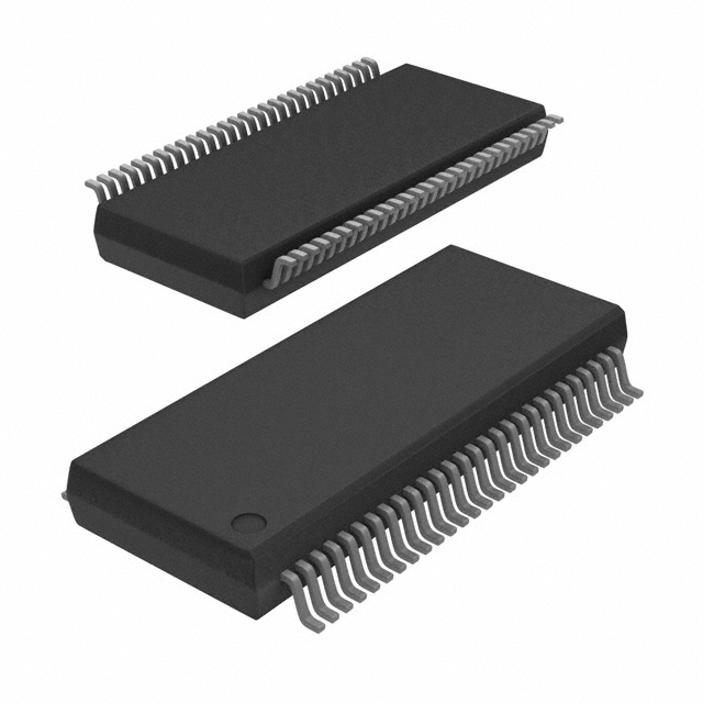
The 74FCT162511CTPVG8 is typically available in a surface-mount package, such as a TSSOP (Thin Shrink Small Outline Package). It is commonly sold in reels or tubes containing multiple units, with quantities varying based on the supplier and customer requirements.
Specifications
- Supply voltage: 4.5V to 5.5V
- Operating temperature range: -40°C to +85°C
- Input/output compatibility: TTL-compatible
- Maximum clock frequency: 100 MHz
- Output drive capability: ±24 mA
- Propagation delay: 6 ns (max)
- Power dissipation: 500 mW (max)
Pin Configuration
The 74FCT162511CTPVG8 has a total of 48 pins, which are assigned specific functions. Here is a detailed pin configuration:
- A0: Input pin for the least significant bit of the data bus.
- A1-A15: Input pins for the remaining bits of the data bus.
- OE (Output Enable): Controls the output state of the device.
- DIR (Direction Control): Determines the direction of data flow.
- CLK (Clock): Input pin for the clock signal.
- D0-D15: Bi-directional data pins.
- GND: Ground reference.
- VCC: Supply voltage.
Note: The remaining pins are not listed here for brevity.
Functional Features
- Bidirectional data transfer: The 74FCT162511CTPVG8 allows data to be transmitted and received on the same set of pins, facilitating efficient communication between devices.
- Register-based operation: The device includes internal registers that store incoming data before transmitting it, ensuring synchronized and reliable data transfer.
- 3-state outputs: The outputs can be put into a high-impedance state, allowing multiple devices to share a common bus without causing conflicts or signal degradation.
- TTL compatibility: The input and output levels are compatible with TTL logic, making it easy to integrate this device into existing systems.
Advantages and Disadvantages
Advantages
- High-speed operation enables rapid data transfer.
- 16-bit capacity allows for processing large amounts of data simultaneously.
- Registered transceiver design ensures reliable data transmission.
- 3-state outputs facilitate bus sharing in complex systems.
- TTL compatibility simplifies integration into existing designs.
Disadvantages
- Limited operating temperature range (-40°C to +85°C) may restrict certain applications.
- Requires careful consideration of power dissipation due to its relatively high power consumption.
- Availability and pricing may vary based on supplier and market demand.
Working Principles
The 74FCT162511CTPVG8 operates based on the principles of digital logic. It utilizes internal registers to store incoming data and synchronizes its output with a clock signal. The direction of data flow is controlled by the DIR pin, while the OE pin enables or disables the outputs. The device's 3-state outputs allow it to share a common bus with other devices without causing conflicts.
Application Field Plans
The 74FCT162511CTPVG8 finds applications in various fields, including but not limited to: - Data communication systems - Computer networks - Microprocessor-based systems - Industrial automation - Telecommunications equipment - Test and measurement instruments
Alternative Models
There are several alternative models available that offer similar functionality to the 74FCT162511CTPVG8. Some notable alternatives include: - SN74FCT162511CTPVG8 - MC74FCT162511CTPVG8 - CD74FCT162511CTPVG8
These alternative models may vary in terms of manufacturer, package type, and minor specifications, but they generally serve the same purpose as the 74FCT162511CTPVG8.
In conclusion
Lista 10 Vanliga frågor och svar relaterade till tillämpningen av 74FCT162511CTPVG8 i tekniska lösningar
Sure! Here are 10 common questions and answers related to the application of 74FCT162511CTPVG8 in technical solutions:
Q: What is the 74FCT162511CTPVG8? A: The 74FCT162511CTPVG8 is a 25-bit registered transceiver with 3-state outputs, designed for high-performance bus interface applications.
Q: What is the maximum operating frequency of the 74FCT162511CTPVG8? A: The maximum operating frequency of the 74FCT162511CTPVG8 is typically around 200 MHz.
Q: What voltage levels does the 74FCT162511CTPVG8 support? A: The 74FCT162511CTPVG8 supports both 3.3V and 5V voltage levels.
Q: Can the 74FCT162511CTPVG8 be used as a bidirectional buffer? A: Yes, the 74FCT162511CTPVG8 can be used as a bidirectional buffer, allowing data to flow in both directions.
Q: How many data bits can the 74FCT162511CTPVG8 handle? A: The 74FCT162511CTPVG8 can handle up to 25 data bits.
Q: Does the 74FCT162511CTPVG8 have built-in output enable functionality? A: Yes, the 74FCT162511CTPVG8 has built-in output enable pins that allow you to control the tri-state outputs.
Q: What is the typical propagation delay of the 74FCT162511CTPVG8? A: The typical propagation delay of the 74FCT162511CTPVG8 is around 3-5 nanoseconds.
Q: Can the 74FCT162511CTPVG8 be used in high-speed data transmission applications? A: Yes, the 74FCT162511CTPVG8 is designed for high-performance applications and can be used in high-speed data transmission.
Q: Does the 74FCT162511CTPVG8 have any built-in ESD protection? A: Yes, the 74FCT162511CTPVG8 has built-in ESD protection to safeguard against electrostatic discharge.
Q: What package options are available for the 74FCT162511CTPVG8? A: The 74FCT162511CTPVG8 is available in various package options, such as TSSOP, SSOP, and TVSOP.
Please note that the answers provided here are general and may vary depending on the specific datasheet and manufacturer's specifications of the 74FCT162511CTPVG8.