

Encyclopedia Entry: 54FCT574ATDB
Product Information Overview
Category: Integrated Circuit (IC)
Use: The 54FCT574ATDB is a high-speed octal D-type flip-flop with tri-state outputs. It is commonly used in digital systems for data storage and transfer operations.
Characteristics: - High-speed operation - Tri-state outputs for bus-oriented applications - Low power consumption - Wide operating voltage range - Compatible with TTL logic levels - RoHS compliant
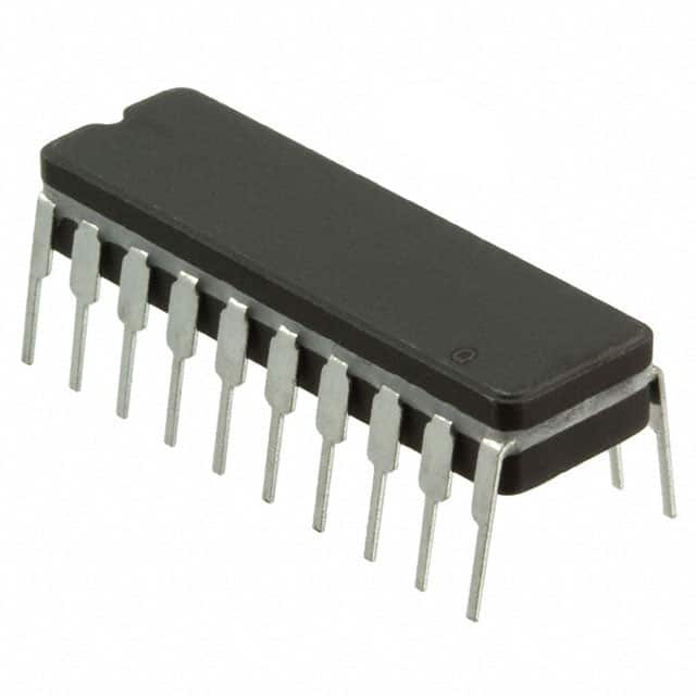
Package: The 54FCT574ATDB is available in a standard 20-pin TSSOP (Thin Shrink Small Outline Package) package, which provides good thermal performance and ease of handling during assembly.
Essence: This IC is designed to provide reliable and efficient data storage and transfer capabilities in various digital systems.
Packaging/Quantity: The 54FCT574ATDB is typically sold in reels or tubes containing multiple units, with each reel/tube containing a specific quantity of ICs. The exact packaging and quantity may vary depending on the supplier.
Specifications
- Supply Voltage Range: 4.5V to 5.5V
- Input Voltage Range: 0V to VCC
- Output Voltage Range: 0V to VCC
- Operating Temperature Range: -40°C to +85°C
- Propagation Delay Time: 3.5ns (typical)
- Output Drive Capability: ±24mA
- Input Capacitance: 4pF (typical)
- Power Dissipation: 500mW (max)
Detailed Pin Configuration
The 54FCT574ATDB has a total of 20 pins, each serving a specific function. The pin configuration is as follows:
- GND (Ground)
- D0 (Data Input 0)
- D1 (Data Input 1)
- D2 (Data Input 2)
- D3 (Data Input 3)
- D4 (Data Input 4)
- D5 (Data Input 5)
- D6 (Data Input 6)
- D7 (Data Input 7)
- OE (Output Enable)
- Q0 (Flip-Flop Output 0)
- Q1 (Flip-Flop Output 1)
- Q2 (Flip-Flop Output 2)
- Q3 (Flip-Flop Output 3)
- Q4 (Flip-Flop Output 4)
- Q5 (Flip-Flop Output 5)
- Q6 (Flip-Flop Output 6)
- Q7 (Flip-Flop Output 7)
- VCC (Supply Voltage)
- GND (Ground)
Functional Features
- High-speed operation: The 54FCT574ATDB is designed to operate at high clock frequencies, making it suitable for applications requiring fast data transfer.
- Tri-state outputs: The tri-state outputs allow multiple devices to share a common bus, enabling efficient communication in bus-oriented systems.
- Low power consumption: This IC is optimized for low power consumption, making it suitable for battery-powered devices and energy-efficient applications.
- Wide operating voltage range: The 54FCT574ATDB can operate within a wide voltage range, providing flexibility in various system designs.
- TTL compatibility: It is compatible with TTL logic levels, allowing seamless integration with existing TTL-based systems.
- RoHS compliant: The IC is manufactured using materials that comply with the Restriction of Hazardous Substances (RoHS) directive, ensuring environmental friendliness.
Advantages and Disadvantages
Advantages: - High-speed operation enables efficient data transfer. - Tri-state outputs facilitate bus-oriented applications. - Low power consumption for energy-efficient designs. - Wide operating voltage range provides flexibility. - TTL compatibility allows easy integration with existing systems.
Disadvantages: - Limited output drive capability may restrict use in certain high-current applications. - The TSSOP package may require careful handling during assembly to avoid damage.
Working Principles
The 54FCT574ATDB operates based on the principles of D-type flip-flops. It stores and transfers data using positive-edge-triggered clock inputs. When the clock signal transitions from low to high, the input data is latched and stored in the flip-flop. The stored data is then available at the outputs until the next clock transition occurs.
Detailed Application Field Plans
The 54FCT574ATDB can be applied in various digital systems that require efficient data storage and transfer capabilities. Some potential application fields include: - Microprocessors and microcontrollers - Data communication systems - Memory modules - Industrial automation systems - Automotive electronics - Consumer electronics
Detailed and Complete Alternative Models
- 74HC574: A similar octal D-type flip-flop
Lista 10 Vanliga frågor och svar relaterade till tillämpningen av 54FCT574ATDB i tekniska lösningar
Sure! Here are 10 common questions and answers related to the application of 54FCT574ATDB in technical solutions:
Q: What is the function of the 54FCT574ATDB? A: The 54FCT574ATDB is an octal D-type flip-flop with tri-state outputs.
Q: What is the operating voltage range for the 54FCT574ATDB? A: The operating voltage range is typically between 4.5V and 5.5V.
Q: Can the 54FCT574ATDB be used in both synchronous and asynchronous applications? A: Yes, the 54FCT574ATDB can be used in both synchronous and asynchronous applications.
Q: How many flip-flops are there in the 54FCT574ATDB? A: The 54FCT574ATDB has 8 flip-flops, making it an octal flip-flop.
Q: What is the maximum clock frequency supported by the 54FCT574ATDB? A: The maximum clock frequency supported is typically around 100 MHz.
Q: Can the outputs of the 54FCT574ATDB be disabled? A: Yes, the outputs of the 54FCT574ATDB can be disabled using the tri-state feature.
Q: What is the typical propagation delay of the 54FCT574ATDB? A: The typical propagation delay is around 5 ns.
Q: Is the 54FCT574ATDB compatible with TTL logic levels? A: Yes, the 54FCT574ATDB is compatible with TTL logic levels.
Q: Can the 54FCT574ATDB be cascaded to increase the number of flip-flops? A: Yes, multiple 54FCT574ATDBs can be cascaded to increase the number of flip-flops.
Q: What is the package type for the 54FCT574ATDB? A: The 54FCT574ATDB is available in a 20-pin TSSOP package.
Please note that these answers are general and may vary depending on the specific datasheet and manufacturer's specifications for the 54FCT574ATDB.