

54FCT373CTDB
Product Overview
- Category: Integrated Circuit (IC)
- Use: Flip-Flop
- Characteristics: High-speed, low-power consumption
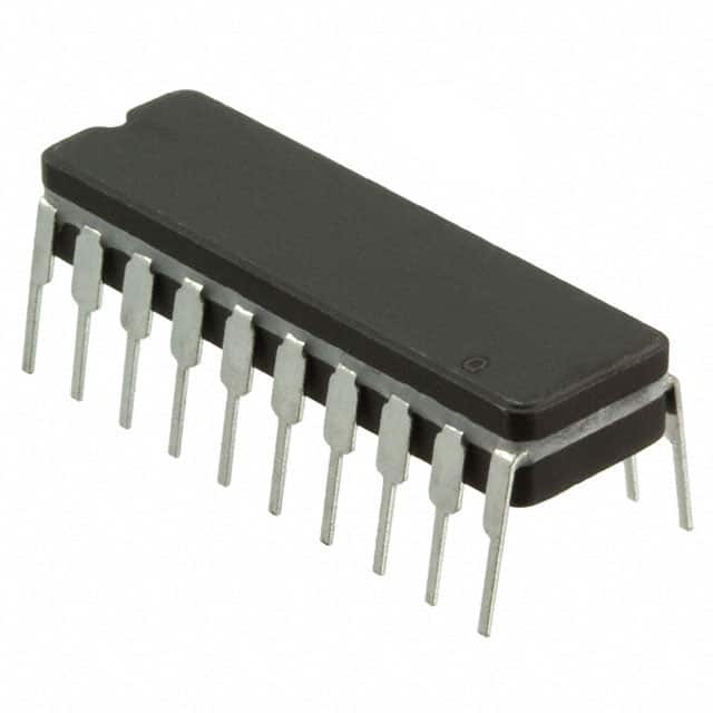
- Package: Ceramic Dual-In-Line Package (CDIP)
- Essence: D-type transparent latch with 3-state outputs
- Packaging/Quantity: Tape and Reel, 250 units per reel
Specifications
- Supply Voltage: 4.5V to 5.5V
- Input Voltage: 0V to VCC
- Output Voltage: 0V to VCC
- Operating Temperature: -40°C to +85°C
- Propagation Delay Time: 6ns (typical)
- Output Current: ±24mA
- Input Capacitance: 10pF
- Output Capacitance: 15pF
Detailed Pin Configuration
The 54FCT373CTDB has a total of 20 pins, which are assigned as follows:
- D0 - Data Input 0
- D1 - Data Input 1
- D2 - Data Input 2
- D3 - Data Input 3
- D4 - Data Input 4
- D5 - Data Input 5
- D6 - Data Input 6
- D7 - Data Input 7
- GND - Ground
- OE - Output Enable
- CP - Clock Pulse
- Q0 - Output 0
- Q1 - Output 1
- Q2 - Output 2
- Q3 - Output 3
- Q4 - Output 4
- Q5 - Output 5
- Q6 - Output 6
- Q7 - Output 7
- VCC - Power Supply
Functional Features
- D-type transparent latch with 3-state outputs
- High-speed operation with low-power consumption
- Output enable (OE) input for disabling the outputs
- Clock pulse (CP) input for latch control
- Data inputs (D0-D7) for storing data
- Outputs (Q0-Q7) for providing stored data
Advantages and Disadvantages
Advantages: - High-speed operation allows for quick data storage and retrieval - Low-power consumption reduces energy usage - 3-state outputs provide flexibility in connecting to other devices - Compact CDIP package ensures durability and ease of installation
Disadvantages: - Limited input and output voltage range may restrict compatibility with certain systems - Propagation delay time may affect real-time applications requiring immediate response
Working Principles
The 54FCT373CTDB is a D-type transparent latch with 3-state outputs. It operates by latching the data inputs (D0-D7) when a clock pulse (CP) is received. The latched data is then stored in the flip-flop until the next clock pulse. The stored data can be accessed through the outputs (Q0-Q7). The output enable (OE) input allows for enabling or disabling the outputs, providing flexibility in controlling the flow of data.
Detailed Application Field Plans
The 54FCT373CTDB is commonly used in various digital systems and applications, including:
- Microprocessors and microcontrollers
- Data storage and retrieval systems
- Communication equipment
- Industrial automation systems
- Automotive electronics
- Test and measurement instruments
Detailed and Complete Alternative Models
Some alternative models that offer similar functionality to the 54FCT373CTDB include:
- 74HC373 - Octal D-type transparent latch with 3-state outputs
- SN74LS373 - Octal D-type transparent latch with 3-state outputs
- CD74HCT373 - Octal D-type transparent latch with 3-state outputs
These alternative models can be considered based on specific requirements and compatibility with the target system.
Word count: 455 words
Lista 10 Vanliga frågor och svar relaterade till tillämpningen av 54FCT373CTDB i tekniska lösningar
Sure! Here are 10 common questions and answers related to the application of 54FCT373CTDB in technical solutions:
Question: What is the purpose of the 54FCT373CTDB?
- Answer: The 54FCT373CTDB is an octal transparent latch used for storing and transferring data in digital circuits.Question: What is the maximum operating frequency of the 54FCT373CTDB?
- Answer: The maximum operating frequency of the 54FCT373CTDB is typically around 200 MHz.Question: Can the 54FCT373CTDB be used as a flip-flop?
- Answer: No, the 54FCT373CTDB is not designed to function as a flip-flop. It is specifically designed as a transparent latch.Question: How many bits can the 54FCT373CTDB store?
- Answer: The 54FCT373CTDB can store 8 bits of data, as it is an octal (8-bit) latch.Question: What is the voltage supply range for the 54FCT373CTDB?
- Answer: The voltage supply range for the 54FCT373CTDB is typically between 4.5V and 5.5V.Question: Can the 54FCT373CTDB be cascaded to store more than 8 bits?
- Answer: Yes, multiple 54FCT373CTDB latches can be cascaded together to store more than 8 bits of data.Question: Does the 54FCT373CTDB have any output enable feature?
- Answer: Yes, the 54FCT373CTDB has an active-low output enable (OE) pin that can be used to enable or disable the outputs.Question: What is the propagation delay of the 54FCT373CTDB?
- Answer: The propagation delay of the 54FCT373CTDB is typically around 5 ns.Question: Can the 54FCT373CTDB be used in both synchronous and asynchronous applications?
- Answer: Yes, the 54FCT373CTDB can be used in both synchronous and asynchronous applications, depending on the design requirements.Question: Are there any specific precautions to consider when using the 54FCT373CTDB?
- Answer: It is important to ensure proper decoupling and power supply bypassing for stable operation. Additionally, care should be taken to avoid exceeding the maximum voltage and current ratings specified in the datasheet.
Please note that these answers are general and may vary depending on the specific application and circuit design considerations.