

PI6C2972FCE
Overview
Product Category
PI6C2972FCE belongs to the category of integrated circuits (ICs).
Use
This product is primarily used for clock and timing applications in electronic devices.
Characteristics
- High precision and accuracy
- Low power consumption
- Wide operating voltage range
- Compact package size
- Easy integration into circuit designs
Package
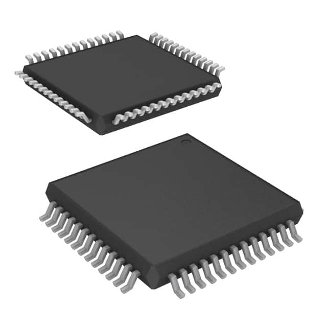
PI6C2972FCE is available in a small form factor package, such as a QFN (Quad Flat No-leads) package.
Essence
The essence of PI6C2972FCE lies in its ability to provide reliable clock and timing signals for various electronic systems.
Packaging/Quantity
Typically, PI6C2972FCE is packaged in reels or trays, with a quantity of 250 or 500 units per reel/tray.
Specifications
- Operating Voltage: 1.8V - 3.3V
- Frequency Range: 1Hz - 100MHz
- Output Types: LVCMOS, LVDS, HCSL
- Temperature Range: -40°C to +85°C
- Supply Current: <10mA
Detailed Pin Configuration
The PI6C2972FCE has a total of 16 pins, which are assigned specific functions as follows:
- VDD: Power supply input
- GND: Ground connection
- CLK_IN: Input clock signal
- CLK_OUT: Output clock signal
- OE: Output enable control
- SEL0: Select input 0
- SEL1: Select input 1
- SEL2: Select input 2
- SEL3: Select input 3
- VDD: Power supply input
- GND: Ground connection
- NC: No connection
- NC: No connection
- NC: No connection
- NC: No connection
- NC: No connection
Functional Features
- Clock signal generation and distribution
- Frequency multiplication and division
- Output enable/disable control
- Selectable input options for versatile applications
- Low jitter and phase noise performance
Advantages and Disadvantages
Advantages
- High precision and accuracy in clock generation
- Wide operating voltage range allows compatibility with various systems
- Low power consumption for energy-efficient designs
- Compact package size enables space-saving integration
- Versatile output types for flexible connectivity options
Disadvantages
- Limited frequency range compared to specialized clock ICs
- May require additional external components for specific applications
Working Principles
PI6C2972FCE operates by receiving an input clock signal (CLKIN) and generating an output clock signal (CLKOUT) based on the selected configuration. The device utilizes internal circuitry to perform frequency multiplication, division, and other timing functions as per the user's requirements. The output enable (OE) pin allows for enabling or disabling the output clock signal.
Detailed Application Field Plans
PI6C2972FCE finds application in various electronic systems that require precise clock and timing signals. Some potential application fields include:
- Communication Systems: Used for synchronization and timing in network switches, routers, and communication modules.
- Consumer Electronics: Integrated into audio/video equipment, gaming consoles, and digital cameras for accurate timing.
- Industrial Automation: Employed in programmable logic controllers (PLCs), motor control systems, and robotics for synchronized operations.
- Automotive Electronics: Utilized in automotive infotainment systems, advanced driver-assistance systems (ADAS), and engine control units (ECUs) for reliable timing.
- Medical Devices: Incorporated into medical imaging equipment, patient monitoring systems, and diagnostic devices to ensure precise timing.
Detailed and Complete Alternative Models
- PI6C557-03QEX: Similar clock IC with extended temperature range (-40°C to +105°C).
- PI6C485-02QEX: Clock IC with enhanced EMI performance for noise-sensitive applications.
- PI6C490-01QEX: Clock IC with additional features like spread spectrum modulation for reduced electromagnetic interference (EMI).
These alternative models offer similar functionality to PI6C2972FCE, catering to specific requirements or operating conditions.
In conclusion, PI6C2972FCE is a versatile clock and timing IC that provides high precision and accuracy in various electronic systems. Its compact size, low power consumption, and wide operating voltage range make it suitable for a wide range of applications. However, designers should consider the limited frequency range and potential need for external components when integrating this IC into their designs.
Lista 10 Vanliga frågor och svar relaterade till tillämpningen av PI6C2972FCE i tekniska lösningar
Question: What is the PI6C2972FCE?
Answer: The PI6C2972FCE is a versatile clock generator and buffer designed for use in technical solutions.Question: What are the key features of the PI6C2972FCE?
Answer: The key features of the PI6C2972FCE include multiple outputs, low jitter, programmable frequency, and wide operating voltage range.Question: How many outputs does the PI6C2972FCE have?
Answer: The PI6C2972FCE has 12 outputs, which can be individually programmed for different frequencies and signal types.Question: What is the operating voltage range of the PI6C2972FCE?
Answer: The PI6C2972FCE operates within a wide voltage range of 1.8V to 3.3V, making it compatible with various systems.Question: Can the PI6C2972FCE generate different clock frequencies simultaneously?
Answer: Yes, the PI6C2972FCE supports simultaneous generation of multiple clock frequencies, allowing for flexible timing solutions.Question: Does the PI6C2972FCE provide any clock skew adjustment capabilities?
Answer: Yes, the PI6C2972FCE offers programmable skew adjustment for fine-tuning the timing of clock signals.Question: Is the PI6C2972FCE suitable for high-speed data communication applications?
Answer: Absolutely, the PI6C2972FCE is designed to meet the requirements of high-speed data communication systems, ensuring reliable signal integrity.Question: Can the PI6C2972FCE be used in battery-powered devices?
Answer: Yes, the PI6C2972FCE's low power consumption makes it suitable for battery-powered devices, extending battery life.Question: Does the PI6C2972FCE support hot-swapping of clock signals?
Answer: Yes, the PI6C2972FCE features hot-swappable clock outputs, allowing for seamless integration and maintenance of clock signals.Question: Are there any application notes or reference designs available for the PI6C2972FCE?
Answer: Yes, the manufacturer provides application notes and reference designs to assist in the implementation of the PI6C2972FCE in various technical solutions.