

74LVC1G98FZ4-7
Product Overview
Category
The 74LVC1G98FZ4-7 belongs to the category of integrated circuits (ICs).
Use
This IC is commonly used in electronic devices for signal switching and routing applications.
Characteristics
- Low-voltage CMOS technology
- High-speed operation
- Wide operating voltage range
- Low power consumption
- Small package size
Package
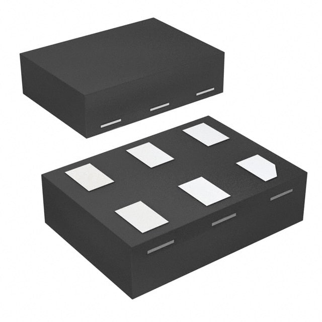
The 74LVC1G98FZ4-7 is available in a small form factor package, typically a surface mount package (SMD). The specific package type may vary depending on the manufacturer.
Essence
The essence of the 74LVC1G98FZ4-7 lies in its ability to efficiently switch and route signals in electronic circuits while consuming minimal power.
Packaging/Quantity
The IC is usually supplied in reels or tubes, with quantities varying based on the manufacturer's packaging specifications.
Specifications
- Supply Voltage: 1.65V to 5.5V
- Input Voltage Range: GND to VCC
- Output Voltage Range: GND to VCC
- Operating Temperature Range: -40°C to +85°C
- Maximum Propagation Delay: 6 ns
- Maximum Quiescent Current: 2 μA
Detailed Pin Configuration
The 74LVC1G98FZ4-7 has a total of 6 pins, which are labeled as follows:
- A - Input A
- B - Input B
- C - Input C
- D - Input D
- Y - Output Y
- GND - Ground
Functional Features
- Quad 2-input multiplexer
- Selects one of four inputs (A, B, C, or D) based on the control inputs
- Provides a single output (Y) that corresponds to the selected input
Advantages and Disadvantages
Advantages
- Low power consumption makes it suitable for battery-powered devices
- Wide operating voltage range allows compatibility with various systems
- High-speed operation enables efficient signal switching
- Small package size saves board space in compact designs
Disadvantages
- Limited number of inputs may not be sufficient for complex applications requiring more inputs
- Propagation delay may introduce timing issues in certain high-speed applications
Working Principles
The 74LVC1G98FZ4-7 operates based on the principles of multiplexing. It uses control inputs to select one of the four input signals and routes it to the output pin. The selection is made by activating the appropriate control inputs, which determine the path for the signal.
Detailed Application Field Plans
The 74LVC1G98FZ4-7 finds application in various electronic devices and systems, including but not limited to: - Consumer electronics - Mobile devices - Automotive electronics - Industrial automation - Communication systems
Detailed and Complete Alternative Models
Some alternative models that can be considered as alternatives to the 74LVC1G98FZ4-7 are: - 74HC1G98 - SN74LVC1G98 - MC74LVC1G98
These models offer similar functionality and characteristics, providing options for designers based on their specific requirements.
In conclusion, the 74LVC1G98FZ4-7 is a versatile integrated circuit used for signal switching and routing applications. Its low power consumption, high-speed operation, and small package size make it suitable for a wide range of electronic devices. However, designers should consider the limited number of inputs and propagation delay when selecting this IC for their applications.
Lista 10 Vanliga frågor och svar relaterade till tillämpningen av 74LVC1G98FZ4-7 i tekniska lösningar
Sure! Here are 10 common questions and answers related to the application of the 74LVC1G98FZ4-7 in technical solutions:
Q1: What is the 74LVC1G98FZ4-7? A1: The 74LVC1G98FZ4-7 is a single-gate configurable multiple function gate IC, commonly used in digital logic circuits.
Q2: What are the key features of the 74LVC1G98FZ4-7? A2: The key features include low power consumption, wide operating voltage range, high-speed operation, and compatibility with both CMOS and TTL logic levels.
Q3: What are the different functions that can be configured using the 74LVC1G98FZ4-7? A3: The 74LVC1G98FZ4-7 can be configured as a 2-input AND gate, 2-input OR gate, 2-input XOR gate, or a 2-input NAND gate.
Q4: What is the maximum operating voltage for the 74LVC1G98FZ4-7? A4: The maximum operating voltage is typically 5.5V.
Q5: Can the 74LVC1G98FZ4-7 be used in battery-powered applications? A5: Yes, the 74LVC1G98FZ4-7's low power consumption makes it suitable for battery-powered applications.
Q6: What is the typical propagation delay of the 74LVC1G98FZ4-7? A6: The typical propagation delay is around 4.5 ns.
Q7: Is the 74LVC1G98FZ4-7 compatible with other logic families? A7: Yes, the 74LVC1G98FZ4-7 is compatible with both CMOS and TTL logic levels.
Q8: Can the 74LVC1G98FZ4-7 be used in high-speed applications? A8: Yes, the 74LVC1G98FZ4-7 is designed for high-speed operation, making it suitable for high-speed applications.
Q9: What is the package type of the 74LVC1G98FZ4-7? A9: The 74LVC1G98FZ4-7 is available in a small SOT353 package.
Q10: Are there any recommended operating conditions for the 74LVC1G98FZ4-7? A10: Yes, some recommended operating conditions include a supply voltage range of 1.65V to 5.5V and an ambient temperature range of -40°C to +125°C.
Please note that the answers provided here are general and may vary depending on the specific datasheet and manufacturer's specifications for the 74LVC1G98FZ4-7.