

74LVC1G34SE-7
Product Overview
Category
The 74LVC1G34SE-7 belongs to the category of integrated circuits (ICs).
Use
This IC is commonly used as a buffer or inverter in various electronic applications.
Characteristics
- Low voltage CMOS technology
- High-speed operation
- Wide operating voltage range
- Schmitt-trigger input for noise immunity
- Small package size
Package
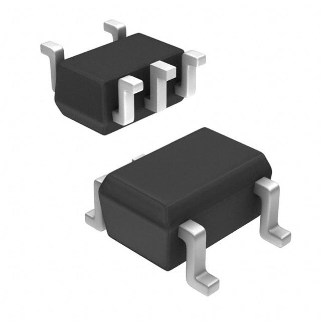
The 74LVC1G34SE-7 is available in a small SOT-353 package.
Essence
The essence of this product lies in its ability to provide buffering and inversion functions in electronic circuits.
Packaging/Quantity
The 74LVC1G34SE-7 is typically packaged in reels, with a quantity of 3000 units per reel.
Specifications
- Supply Voltage Range: 1.65V to 5.5V
- Input Voltage Range: -0.5V to VCC + 0.5V
- Output Voltage Range: -0.5V to VCC + 0.5V
- Operating Temperature Range: -40°C to +125°C
- Maximum Propagation Delay: 4.3 ns at 3.3V supply voltage
Detailed Pin Configuration
The 74LVC1G34SE-7 has the following pin configuration:
____
   A |1    6| VCC
   B |2    5| Y
 GND |3    4| OE
       ----
Functional Features
- Buffering: The 74LVC1G34SE-7 can be used to amplify and stabilize digital signals.
- Inversion: It can invert the logic level of an input signal.
- Noise Immunity: The Schmitt-trigger input provides improved noise immunity, making it suitable for noisy environments.
- High-Speed Operation: The IC operates at high speeds, enabling efficient signal processing.
Advantages and Disadvantages
Advantages
- Low voltage operation allows compatibility with a wide range of systems.
- Small package size saves board space in compact designs.
- Schmitt-trigger input enhances noise immunity, ensuring reliable operation.
Disadvantages
- Limited output current capability may restrict its use in certain applications.
- Single-channel design limits its versatility compared to multi-channel alternatives.
Working Principles
The 74LVC1G34SE-7 utilizes CMOS technology to achieve low voltage operation. It consists of a buffer/inverter circuit that amplifies or inverts the input signal based on the logic level. The Schmitt-trigger input ensures stable operation even in the presence of noise.
Detailed Application Field Plans
The 74LVC1G34SE-7 finds applications in various electronic systems, including but not limited to: - Battery-powered devices - Portable consumer electronics - Industrial control systems - Communication equipment - Automotive electronics
Detailed and Complete Alternative Models
Some alternative models that can be considered as replacements for the 74LVC1G34SE-7 include: - SN74LVC1G34DBVR - MC74VHC1G34DTT1G - TC7SZ34FU
These alternatives offer similar functionality and characteristics, providing flexibility in design choices.
In conclusion, the 74LVC1G34SE-7 is a versatile integrated circuit that serves as a buffer or inverter in various electronic applications. Its low voltage operation, small package size, and noise immunity make it suitable for a wide range of systems. While it has some limitations in terms of output current and channel count, there are alternative models available to meet specific requirements.
Lista 10 Vanliga frågor och svar relaterade till tillämpningen av 74LVC1G34SE-7 i tekniska lösningar
Sure! Here are 10 common questions and answers related to the application of 74LVC1G34SE-7 in technical solutions:
Q: What is the 74LVC1G34SE-7? A: The 74LVC1G34SE-7 is a single buffer gate with Schmitt-trigger inputs, which is commonly used in digital logic circuits.
Q: What is the purpose of a buffer gate? A: A buffer gate is used to isolate or amplify signals in a digital circuit, ensuring proper signal integrity and driving capability.
Q: What are Schmitt-trigger inputs? A: Schmitt-trigger inputs provide hysteresis, meaning they have different voltage thresholds for rising and falling edges, making them less susceptible to noise.
Q: What is the operating voltage range of the 74LVC1G34SE-7? A: The 74LVC1G34SE-7 operates within a voltage range of 1.65V to 5.5V.
Q: What is the maximum output current of the 74LVC1G34SE-7? A: The 74LVC1G34SE-7 can source or sink up to 32mA of current.
Q: Can the 74LVC1G34SE-7 be used as a level shifter? A: Yes, the 74LVC1G34SE-7 can be used as a level shifter to convert signals between different voltage levels.
Q: Is the 74LVC1G34SE-7 suitable for high-speed applications? A: Yes, the 74LVC1G34SE-7 has a propagation delay of only a few nanoseconds, making it suitable for high-speed applications.
Q: Can the 74LVC1G34SE-7 be used in battery-powered devices? A: Yes, the 74LVC1G34SE-7 has a low power consumption and can be used in battery-powered devices.
Q: Does the 74LVC1G34SE-7 have built-in ESD protection? A: Yes, the 74LVC1G34SE-7 is designed with built-in ESD protection to prevent damage from electrostatic discharge.
Q: What package options are available for the 74LVC1G34SE-7? A: The 74LVC1G34SE-7 is available in various package options, such as SOT353, SC-88A, and XSON6.