

Encyclopedia Entry: 74AHCT1G00SE-7
Product Overview
Category
The 74AHCT1G00SE-7 belongs to the category of integrated circuits (ICs).
Use
This product is commonly used in electronic devices and circuits for signal amplification, switching, and logic operations.
Characteristics
- The 74AHCT1G00SE-7 is a single 2-input NAND gate.
- It operates at high-speed with low power consumption.
- The IC has a wide operating voltage range and can tolerate high noise immunity.
- It is designed to be compatible with both TTL and CMOS logic families.
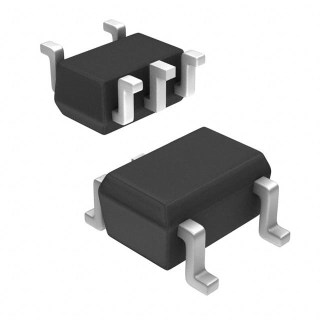
Package
The 74AHCT1G00SE-7 is available in a small surface-mount package (SOT-353) which consists of three pins.
Essence
The essence of this product lies in its ability to perform logical operations efficiently and reliably within electronic circuits.
Packaging/Quantity
The 74AHCT1G00SE-7 is typically packaged in reels or tubes, containing a specific quantity of ICs per package. The exact quantity may vary depending on the manufacturer's specifications.
Specifications
- Supply Voltage Range: 2.0V to 5.5V
- Input Voltage Range: 0V to VCC
- Output Voltage Range: 0V to VCC
- Operating Temperature Range: -40°C to +85°C
- Propagation Delay Time: 4.5ns (typical)
Detailed Pin Configuration
The 74AHCT1G00SE-7 has three pins arranged as follows:
____
   A --|    |-- VCC
   B --|    |-- Y
 GND --|____|-- NC
- A: Input A
- B: Input B
- VCC: Power supply voltage
- Y: Output
- GND: Ground
- NC: No connection
Functional Features
- The 74AHCT1G00SE-7 performs the logical NAND operation on its two input signals (A and B).
- It provides a single output signal (Y) that is the logical complement of the NAND operation.
- The IC operates at high speed, making it suitable for applications requiring quick response times.
- It has a wide operating voltage range, allowing compatibility with various power supply levels.
- The 74AHCT1G00SE-7 exhibits high noise immunity, ensuring reliable operation in noisy environments.
Advantages and Disadvantages
Advantages
- High-speed operation
- Low power consumption
- Wide operating voltage range
- Compatibility with TTL and CMOS logic families
- High noise immunity
Disadvantages
- Limited functionality as a single NAND gate
- May require additional components for complex logic operations
Working Principles
The 74AHCT1G00SE-7 utilizes semiconductor technology to implement the NAND gate function. It consists of transistors and resistors arranged in a specific configuration to achieve the desired logical operation. When the input signals A and B are applied, the internal circuitry processes these signals and generates the corresponding output signal Y based on the NAND truth table.
Detailed Application Field Plans
The 74AHCT1G00SE-7 finds application in various electronic systems, including but not limited to: - Digital logic circuits - Microcontrollers - Data communication devices - Industrial automation systems - Consumer electronics
Detailed and Complete Alternative Models
- 74HC00: Quad 2-input NAND gate
- SN74LS00: Quad 2-input NAND gate
- CD4011: Quad 2-input NAND gate
- MC14011: Quad 2-input NAND gate
- HCF4011: Quad 2-input NAND gate
These alternative models offer similar functionality to the 74AHCT1G00SE-7 and can be used as substitutes depending on specific requirements.
In conclusion, the 74AHCT1G00SE-7 is a versatile integrated circuit that serves as a single 2-input NAND gate. Its high-speed operation, low power consumption, and compatibility with various logic families make it an essential component in numerous electronic applications.
Lista 10 Vanliga frågor och svar relaterade till tillämpningen av 74AHCT1G00SE-7 i tekniska lösningar
Sure! Here are 10 common questions and answers related to the application of 74AHCT1G00SE-7 in technical solutions:
Q1: What is the 74AHCT1G00SE-7? A1: The 74AHCT1G00SE-7 is a single 2-input NAND gate IC (integrated circuit) that operates on a supply voltage range of 4.5V to 5.5V.
Q2: What is the purpose of a NAND gate? A2: A NAND gate is a logic gate that performs the logical operation of the Boolean NAND function. It produces an output that is the inverse of the logical AND of its input signals.
Q3: What are some typical applications of the 74AHCT1G00SE-7? A3: The 74AHCT1G00SE-7 can be used in various applications such as digital logic circuits, signal processing, data communication systems, and control systems.
Q4: What is the maximum operating frequency of the 74AHCT1G00SE-7? A4: The maximum operating frequency of the 74AHCT1G00SE-7 is typically around 200 MHz.
Q5: What is the power consumption of the 74AHCT1G00SE-7? A5: The power consumption of the 74AHCT1G00SE-7 is relatively low, making it suitable for battery-powered devices or applications where power efficiency is important.
Q6: Can the 74AHCT1G00SE-7 drive other ICs directly? A6: Yes, the 74AHCT1G00SE-7 has a high output current capability, allowing it to drive other ICs directly without the need for additional buffer circuits.
Q7: What is the input voltage range of the 74AHCT1G00SE-7? A7: The input voltage range of the 74AHCT1G00SE-7 is compatible with standard TTL (Transistor-Transistor Logic) and CMOS (Complementary Metal-Oxide-Semiconductor) logic levels.
Q8: Can the 74AHCT1G00SE-7 be used in both digital and analog circuits? A8: No, the 74AHCT1G00SE-7 is primarily designed for digital logic applications and may not be suitable for precise analog signal processing.
Q9: Is the 74AHCT1G00SE-7 available in different package options? A9: Yes, the 74AHCT1G00SE-7 is available in various package options such as SOT23, SC-70, and XSON.
Q10: Are there any special considerations when using the 74AHCT1G00SE-7 in high-speed applications? A10: In high-speed applications, it is important to consider factors such as signal integrity, PCB layout, and proper decoupling to ensure reliable operation of the 74AHCT1G00SE-7.