

CY7C4245V-15ASXC
Product Overview
Category
The CY7C4245V-15ASXC belongs to the category of integrated circuits (ICs), specifically a synchronous dual-port static random access memory (SDP SRAM) chip.
Use
This IC is primarily used in applications that require high-speed and reliable data storage and retrieval. It provides simultaneous read and write operations on two independent ports, making it suitable for various data-intensive systems.
Characteristics
- Synchronous operation: The CY7C4245V-15ASXC operates synchronously with an external clock signal, ensuring precise timing and efficient data transfer.
- Dual-port architecture: It features two independent ports, allowing simultaneous access from different sources without any conflicts.
- High-speed performance: With a maximum operating frequency of 150 MHz, this IC offers fast data transfer rates, enabling real-time processing in demanding applications.
- Low power consumption: The CY7C4245V-15ASXC is designed to minimize power consumption, making it suitable for battery-powered devices or energy-efficient systems.
- Wide voltage range: It supports a wide supply voltage range, typically from 3.0V to 3.6V, providing flexibility in various electronic designs.
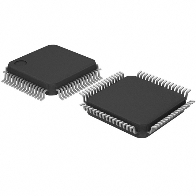
Package and Quantity
The CY7C4245V-15ASXC is available in a small outline integrated circuit (SOIC) package. Each package contains one IC.
Specifications
- Memory capacity: 4 Megabits (512K x 8 bits)
- Access time: 15 ns
- Operating voltage: 3.0V - 3.6V
- Operating temperature range: -40°C to +85°C
- Package type: SOIC-28
Pin Configuration
The CY7C4245V-15ASXC has a total of 28 pins, which are assigned specific functions. The pin configuration is as follows:
```
Pin Name Function
1 A0-A18 Address Inputs 2 CE1 Chip Enable Port 1 3 CE2 Chip Enable Port 2 4 OE Output Enable 5 WE Write Enable 6 LB Lower Byte Control 7 UB Upper Byte Control 8 GND Ground 9 DQ0-DQ7 Data Input/Output 10 VCC Power Supply 11 CLK Clock Input 12 A19 Address Input 13 A20 Address Input 14 A21 Address Input 15 A22 Address Input 16 A23 Address Input 17 A24 Address Input 18 A25 Address Input 19 A26 Address Input 20 A27 Address Input 21 A28 Address Input 22 A29 Address Input 23 A30 Address Input 24 A31 Address Input 25 A32 Address Input 26 A33 Address Input 27 A34 Address Input 28 VCC Power Supply ```
Functional Features
- Simultaneous read and write: The CY7C4245V-15ASXC allows independent read and write operations on both ports simultaneously, enabling efficient data transfer between different devices or subsystems.
- Asynchronous and synchronous operation: It supports both asynchronous and synchronous modes of operation, providing flexibility in various system architectures.
- Byte control functionality: The lower byte (LB) and upper byte (UB) control pins allow selective reading or writing of individual bytes, enhancing versatility in data manipulation.
Advantages and Disadvantages
Advantages
- Dual-port architecture enables simultaneous access from multiple sources without conflicts.
- High-speed operation facilitates real-time data processing.
- Low power consumption makes it suitable for energy-efficient applications.
- Wide voltage range provides flexibility in electronic designs.
Disadvantages
- Limited memory capacity compared to higher-density SRAM chips.
- Relatively higher cost per megabit compared to larger memory devices.
Working Principles
The CY7C4245V-15ASXC operates based on the principles of synchronous static random access memory. It stores and retrieves data using a combination of address inputs, control signals, and clock synchronization. The dual-port architecture allows independent read and write operations on two separate ports, ensuring efficient data transfer between different components or subsystems.
Detailed Application Field Plans
The CY7C4245V-15ASXC finds application in various fields that require high-speed and reliable data storage and retrieval. Some potential application areas include: 1. Networking equipment: Used in routers, switches, and network interface cards to store routing tables, packet buffers, and other critical data. 2. Telecommunications systems: Employed in base stations, voice/data switches, and transmission equipment for buffering and caching purposes. 3. Industrial automation:
Lista 10 Vanliga frågor och svar relaterade till tillämpningen av CY7C4245V-15ASXC i tekniska lösningar
Sure! Here are 10 common questions and answers related to the application of CY7C4245V-15ASXC in technical solutions:
Question: What is the maximum operating frequency of CY7C4245V-15ASXC?
Answer: The maximum operating frequency of CY7C4245V-15ASXC is 133 MHz.Question: What is the voltage supply range for CY7C4245V-15ASXC?
Answer: The voltage supply range for CY7C4245V-15ASXC is 3.0V to 3.6V.Question: Can CY7C4245V-15ASXC be used as a bidirectional level shifter?
Answer: Yes, CY7C4245V-15ASXC can be used as a bidirectional level shifter for various applications.Question: What is the typical propagation delay of CY7C4245V-15ASXC?
Answer: The typical propagation delay of CY7C4245V-15ASXC is 8 ns.Question: Does CY7C4245V-15ASXC support hot insertion?
Answer: Yes, CY7C4245V-15ASXC supports hot insertion, allowing for easy plug-and-play functionality.Question: Can CY7C4245V-15ASXC be used in automotive applications?
Answer: Yes, CY7C4245V-15ASXC is suitable for automotive applications due to its wide temperature range and robust design.Question: What is the maximum data rate supported by CY7C4245V-15ASXC?
Answer: The maximum data rate supported by CY7C4245V-15ASXC is 266 Mbps.Question: Does CY7C4245V-15ASXC have built-in ESD protection?
Answer: Yes, CY7C4245V-15ASXC has built-in ESD protection, ensuring reliable operation in harsh environments.Question: Can CY7C4245V-15ASXC be used in low-power applications?
Answer: Yes, CY7C4245V-15ASXC is designed for low-power applications, consuming minimal power during operation.Question: Is CY7C4245V-15ASXC compatible with other logic families?
Answer: Yes, CY7C4245V-15ASXC is compatible with various logic families, making it versatile for different system designs.
Please note that these answers are based on general information and it's always recommended to refer to the datasheet and consult with technical experts for specific application requirements.