

CY7C4225V-15ASC
Product Overview
Category
The CY7C4225V-15ASC belongs to the category of integrated circuits (ICs), specifically a synchronous static random access memory (SRAM) chip.
Use
This SRAM chip is commonly used in various electronic devices and systems that require high-speed and reliable data storage and retrieval capabilities.
Characteristics
- High-speed operation: The CY7C4225V-15ASC offers fast access times, allowing for efficient data processing.
- Large storage capacity: This chip has a storage capacity of 256 kilobits (32 kilobytes), providing ample space for data storage.
- Synchronous interface: It features a synchronous interface, enabling synchronized communication with other components in the system.
- Low power consumption: The CY7C4225V-15ASC is designed to operate with low power consumption, making it suitable for battery-powered devices.
- Wide operating voltage range: It can operate within a wide voltage range, ensuring compatibility with different power supply configurations.
Package and Quantity
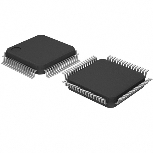
The CY7C4225V-15ASC is available in a small outline integrated circuit (SOIC) package. It is typically sold in reels or tubes, with a quantity of 250 units per reel/tube.
Specifications
- Organization: 32K x 8 bits
- Access Time: 15 ns
- Operating Voltage: 3.3V
- Standby Current: 10 µA (maximum)
- Operating Temperature Range: -40°C to +85°C
- Package Type: SOIC-28
Pin Configuration
The CY7C4225V-15ASC has a total of 28 pins, which are assigned specific functions as follows:
- Chip Enable (CE)
- Output Enable (OE)
- Write Enable (WE)
- Address Inputs (A0-A14)
- Data Inputs/Outputs (DQ0-DQ7)
- Power Supply (VCC)
- Ground (GND)
The remaining pins are used for power supply and ground connections.
Functional Features
- Asynchronous and synchronous operation modes: The CY7C4225V-15ASC can be operated in both asynchronous and synchronous modes, providing flexibility in different system configurations.
- Burst mode support: It supports burst read and write operations, allowing for efficient data transfer between the SRAM and other components.
- Automatic power-down: The chip includes a power-down feature that reduces power consumption when not in use, extending battery life in portable devices.
- Built-in error detection and correction: It incorporates error detection and correction circuitry to ensure data integrity and reliability.
Advantages and Disadvantages
Advantages
- High-speed operation enables fast data access and processing.
- Large storage capacity accommodates significant amounts of data.
- Low power consumption makes it suitable for energy-efficient applications.
- Wide operating voltage range enhances compatibility with various power supply configurations.
- Error detection and correction feature ensures data integrity.
Disadvantages
- Relatively higher cost compared to other types of memory chips with similar capacities.
- Limited availability in certain markets due to specific package type and quantity options.
Working Principles
The CY7C4225V-15ASC operates based on the principles of static random access memory. It stores data in a volatile manner, meaning that the stored information is lost when power is removed. The chip utilizes a combination of transistors and capacitors to store and retrieve data quickly and efficiently.
When powered on, the chip initializes its internal circuitry and becomes ready to receive commands and data. The address inputs are used to specify the location in memory where data needs to be read from or written to. The control signals, such as Chip Enable (CE), Output Enable (OE), and Write Enable (WE), determine the type of operation to be performed.
During read operations, the requested data is retrieved from the specified memory location and made available on the data outputs. Conversely, during write operations, data provided on the data inputs is stored in the designated memory location.
Detailed Application Field Plans
The CY7C4225V-15ASC finds applications in various electronic systems that require high-speed and reliable data storage capabilities. Some potential application fields include:
- Computer Systems: The chip can be used in computer systems as cache memory or for storing critical system data.
- Networking Equipment: It can be employed in routers, switches, and other networking devices to store routing tables and temporary data buffers.
- Industrial Control Systems: The SRAM chip can be utilized in industrial control systems for storing real-time sensor data and program code.
- Communication Devices: It can be integrated into communication devices such as modems and wireless transceivers to facilitate data buffering and processing.
Alternative Models
In addition to the CY7C4225V-15ASC, there are several alternative
Lista 10 Vanliga frågor och svar relaterade till tillämpningen av CY7C4225V-15ASC i tekniska lösningar
Sure! Here are 10 common questions and answers related to the application of CY7C4225V-15ASC in technical solutions:
Q: What is the CY7C4225V-15ASC? A: The CY7C4225V-15ASC is a high-speed, low-power synchronous SRAM (Static Random Access Memory) with a capacity of 256K x 18 bits.
Q: What are the key features of CY7C4225V-15ASC? A: Some key features include a 15 ns access time, 3.3V power supply, 18-bit wide data bus, and a maximum operating frequency of 66 MHz.
Q: What are the typical applications of CY7C4225V-15ASC? A: This SRAM is commonly used in networking equipment, telecommunications systems, industrial automation, and other high-performance computing applications.
Q: How does CY7C4225V-15ASC differ from other SRAMs? A: CY7C4225V-15ASC stands out due to its high-speed operation, low power consumption, and large capacity, making it suitable for demanding applications.
Q: Can I use CY7C4225V-15ASC in battery-powered devices? A: Yes, the low-power design of CY7C4225V-15ASC makes it suitable for battery-powered devices where power efficiency is crucial.
Q: What is the voltage range supported by CY7C4225V-15ASC? A: CY7C4225V-15ASC operates with a 3.3V power supply, which is within the standard voltage range for most digital systems.
Q: Does CY7C4225V-15ASC support multiple read/write operations simultaneously? A: Yes, CY7C4225V-15ASC supports simultaneous read and write operations on different memory locations, allowing for efficient data access.
Q: Can I interface CY7C4225V-15ASC with microcontrollers or processors? A: Absolutely! CY7C4225V-15ASC can be easily interfaced with various microcontrollers, processors, and other digital devices using standard bus protocols.
Q: What is the operating temperature range of CY7C4225V-15ASC? A: The operating temperature range for CY7C4225V-15ASC is typically -40°C to +85°C, making it suitable for a wide range of environments.
Q: Are there any specific design considerations when using CY7C4225V-15ASC? A: It is important to ensure proper decoupling capacitors, signal integrity, and timing requirements are met to maximize the performance of CY7C4225V-15ASC in your design.
Please note that these answers are general and may vary depending on the specific application and requirements.