

CY7C1041G30-10ZSXE
Product Overview
Category
The CY7C1041G30-10ZSXE belongs to the category of synchronous static random access memory (SRAM) chips.
Use
This product is primarily used in electronic devices and systems that require high-speed and reliable data storage and retrieval capabilities.
Characteristics
- Synchronous operation: The CY7C1041G30-10ZSXE operates synchronously with the system clock, allowing for efficient data transfer.
- High-speed performance: With a maximum operating frequency of 100 MHz, this SRAM chip offers fast read and write operations.
- Low power consumption: The CY7C1041G30-10ZSXE is designed to minimize power consumption, making it suitable for battery-powered devices.
- High density: This chip has a capacity of 4 megabits (512K x 8), providing ample storage space for data-intensive applications.
- Wide voltage range: It supports a voltage range of 2.3V to 3.6V, ensuring compatibility with various system configurations.
Package
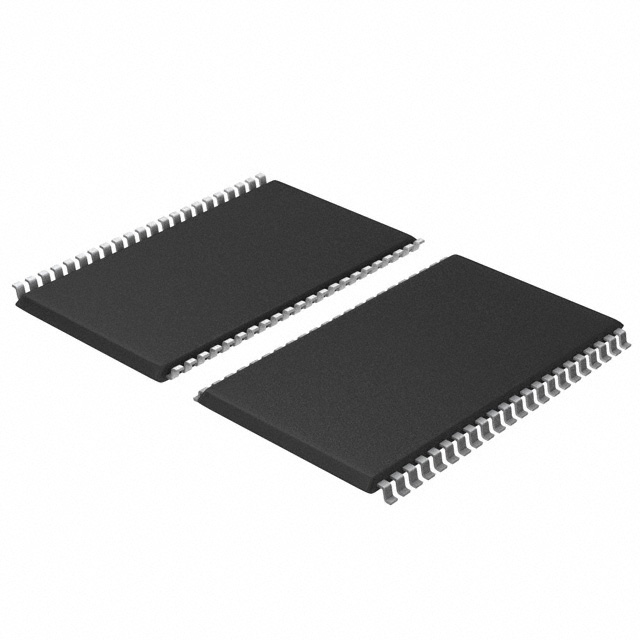
The CY7C1041G30-10ZSXE is available in a small-outline integrated circuit (SOIC) package, which provides ease of integration into circuit boards.
Essence
The essence of the CY7C1041G30-10ZSXE lies in its ability to provide high-speed and reliable data storage in a compact form factor, making it an essential component in modern electronic devices.
Packaging/Quantity
This SRAM chip is typically packaged in reels or trays, with each reel containing a specific quantity of chips. The exact packaging and quantity may vary depending on the supplier.
Specifications
- Organization: 512K x 8 bits
- Operating Voltage: 2.3V - 3.6V
- Operating Frequency: Up to 100 MHz
- Access Time: 10 ns
- Standby Current: 5 μA (typical)
- Package Type: SOIC
Detailed Pin Configuration
The CY7C1041G30-10ZSXE has a total of 32 pins, which are assigned specific functions. The pin configuration is as follows:
```
Pin Name Function
1 VCC Power Supply 2 A12 Address Input 3 A7 Address Input 4 A6 Address Input 5 A5 Address Input 6 A4 Address Input 7 A3 Address Input 8 A2 Address Input 9 A1 Address Input 10 A0 Address Input 11 WE# Write Enable 12 OE# Output Enable 13 I/O0 Data Input/Output 14 I/O1 Data Input/Output 15 I/O2 Data Input/Output 16 I/O3 Data Input/Output 17 I/O4 Data Input/Output 18 I/O5 Data Input/Output 19 I/O6 Data Input/Output 20 I/O7 Data Input/Output 21 GND Ground 22 NC No Connection 23 NC No Connection 24 NC No Connection 25 NC No Connection 26 NC No Connection 27 NC No Connection 28 NC No Connection 29 NC No Connection 30 NC No Connection 31 NC No Connection 32 VCC Power Supply ```
Functional Features
- High-speed data access: The CY7C1041G30-10ZSXE offers fast read and write operations, enabling efficient data access in time-critical applications.
- Synchronous operation: This SRAM chip synchronizes its operations with the system clock, ensuring reliable and accurate data transfer.
- Low power consumption: With its optimized design, the CY7C1041G30-10ZSXE minimizes power consumption, making it suitable for energy-efficient devices.
- Easy integration: The small-outline integrated circuit (SOIC) package allows for easy integration into circuit boards, simplifying the overall design process.
Advantages and Disadvantages
Advantages
- High-speed performance enables quick data access.
- Low power consumption prolongs battery life in portable devices.
- Wide voltage range ensures compatibility with various system configurations.
- Compact form factor facilitates easy integration into circuit boards.
Disadvantages
- Limited storage capacity compared to higher-density memory chips.
- Relatively higher cost per megabit compared to other memory technologies.
Working Principles
The CY7C1041G30-10ZSXE operates based on the principles of synchronous static random access memory (SRAM). It stores data in a volatile manner, meaning that
Lista 10 Vanliga frågor och svar relaterade till tillämpningen av CY7C1041G30-10ZSXE i tekniska lösningar
Sure! Here are 10 common questions and answers related to the application of CY7C1041G30-10ZSXE in technical solutions:
Q1: What is the CY7C1041G30-10ZSXE? A1: The CY7C1041G30-10ZSXE is a high-speed synchronous SRAM (Static Random Access Memory) chip manufactured by Cypress Semiconductor.
Q2: What is the capacity of the CY7C1041G30-10ZSXE? A2: The CY7C1041G30-10ZSXE has a capacity of 4 Megabits (512K x 8 bits).
Q3: What is the operating voltage range for the CY7C1041G30-10ZSXE? A3: The operating voltage range for the CY7C1041G30-10ZSXE is 3.0V to 3.6V.
Q4: What is the maximum operating frequency of the CY7C1041G30-10ZSXE? A4: The CY7C1041G30-10ZSXE can operate at a maximum frequency of 100 MHz.
Q5: What is the access time of the CY7C1041G30-10ZSXE? A5: The access time of the CY7C1041G30-10ZSXE is 10 ns.
Q6: Does the CY7C1041G30-10ZSXE support burst mode operation? A6: Yes, the CY7C1041G30-10ZSXE supports burst mode operation with programmable burst lengths.
Q7: Can the CY7C1041G30-10ZSXE be used in industrial applications? A7: Yes, the CY7C1041G30-10ZSXE is suitable for industrial applications as it operates in a wide temperature range (-40°C to +85°C).
Q8: What are the package options available for the CY7C1041G30-10ZSXE? A8: The CY7C1041G30-10ZSXE is available in a 32-pin TSOP (Thin Small Outline Package) and a 48-ball VFBGA (Very Fine Pitch Ball Grid Array) package.
Q9: Does the CY7C1041G30-10ZSXE have any power-saving features? A9: Yes, the CY7C1041G30-10ZSXE has various power-saving features such as deep power-down mode and automatic power-down.
Q10: Can the CY7C1041G30-10ZSXE be used in battery-powered devices? A10: Yes, the CY7C1041G30-10ZSXE can be used in battery-powered devices as it has low power consumption and power-saving features.
Please note that these answers are based on general information about the CY7C1041G30-10ZSXE and may vary depending on specific application requirements.