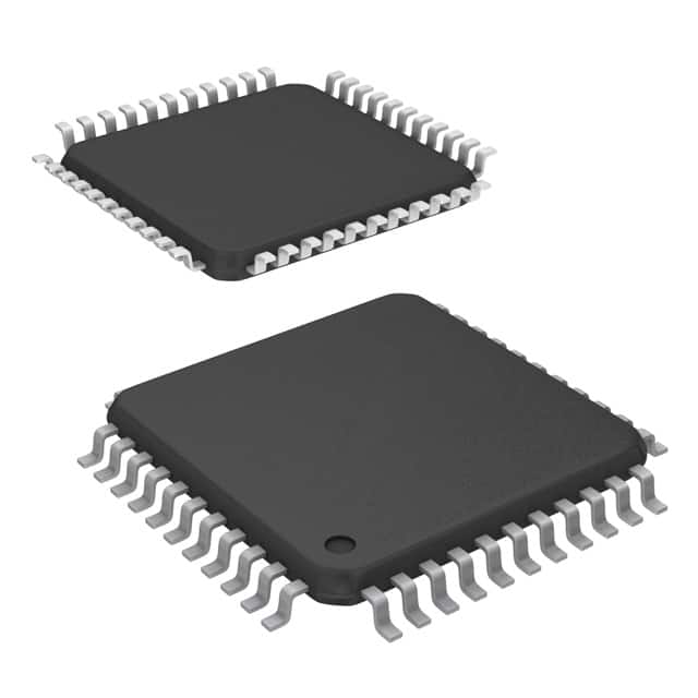
CY7B995AXIT
Product Overview
Category
CY7B995AXIT belongs to the category of integrated circuits (ICs).
Use
This product is commonly used in electronic devices for signal conditioning and clock distribution.
Characteristics
- Signal conditioning: CY7B995AXIT provides high-speed, low-jitter signal conditioning capabilities.
- Clock distribution: It efficiently distributes clock signals to multiple components within a system.
- Package: The product comes in a small outline integrated circuit (SOIC) package.
- Essence: CY7B995AXIT is designed to enhance the performance and reliability of electronic systems.
- Packaging/Quantity: It is typically sold in reels containing a specified quantity of units.
Specifications
The specifications of CY7B995AXIT are as follows:
- Supply voltage: 3.3V
- Operating temperature range: -40°C to +85°C
- Input frequency range: 1 MHz to 200 MHz
- Output frequency range: 1 MHz to 200 MHz
- Number of outputs: 10
- Output type: LVCMOS
Detailed Pin Configuration
The pin configuration of CY7B995AXIT is as follows:
- VDD
- GND
- CLKIN
- OE
- Q0
- Q1
- Q2
- Q3
- Q4
- Q5
- Q6
- Q7
- Q8
- Q9
Functional Features
CY7B995AXIT offers the following functional features:
- High-speed signal conditioning: It ensures accurate and reliable signal transmission.
- Low-jitter clock distribution: It minimizes timing errors and improves system synchronization.
- Multiple outputs: The product provides ten output channels for versatile connectivity options.
- Output enable control: The OE pin allows users to enable or disable the outputs as needed.
Advantages and Disadvantages
Advantages
- High-speed signal conditioning improves overall system performance.
- Low-jitter clock distribution enhances timing accuracy.
- Multiple output channels offer flexibility in system design.
Disadvantages
- Limited input and output frequency range (1 MHz to 200 MHz).
- Requires external power supply (3.3V).
Working Principles
CY7B995AXIT operates by receiving an input clock signal (CLKIN) and conditioning it to reduce noise and improve signal integrity. The conditioned signal is then distributed to the ten output channels. The OE pin controls the enable/disable state of the outputs.
Detailed Application Field Plans
CY7B995AXIT finds applications in various electronic systems, including:
- Communication equipment: Used for clock distribution in routers, switches, and network devices.
- Test and measurement instruments: Ensures accurate timing in oscilloscopes, logic analyzers, etc.
- Data storage systems: Provides reliable clock signals in hard drives and solid-state drives.
- Industrial automation: Used for synchronization in PLCs, motor control systems, and robotics.
- Automotive electronics: Enhances signal integrity in infotainment systems and advanced driver-assistance systems.
Detailed and Complete Alternative Models
Some alternative models that serve similar purposes to CY7B995AXIT are:
- CY7B9910-5SXI: Offers 10 output channels with LVCMOS output type.
- CDCLVC1106PWR: Provides 6 output channels with a wider frequency range.
- SN74LVC1G3157DCKR: Single-channel switch with voltage level translation capabilities.
These alternative models can be considered based on specific requirements and system constraints.
Word count: 496 words
Lista 10 Vanliga frågor och svar relaterade till tillämpningen av CY7B995AXIT i tekniska lösningar
Sure! Here are 10 common questions and answers related to the application of CY7B995AXIT in technical solutions:
Question: What is CY7B995AXIT?
Answer: CY7B995AXIT is a high-performance, low-skew, low-jitter clock buffer designed for use in various technical solutions.Question: What are the key features of CY7B995AXIT?
Answer: Some key features of CY7B995AXIT include low output skew, low additive jitter, wide input frequency range, and multiple outputs.Question: In what applications can CY7B995AXIT be used?
Answer: CY7B995AXIT can be used in applications such as telecommunications, networking, data centers, and high-speed digital systems.Question: How many outputs does CY7B995AXIT have?
Answer: CY7B995AXIT has 10 outputs, making it suitable for driving multiple devices simultaneously.Question: What is the input frequency range of CY7B995AXIT?
Answer: The input frequency range of CY7B995AXIT is typically between 8 kHz and 200 MHz.Question: Does CY7B995AXIT support different voltage levels?
Answer: Yes, CY7B995AXIT supports both LVCMOS and LVTTL voltage levels.Question: Can CY7B995AXIT be cascaded with other clock buffers?
Answer: Yes, CY7B995AXIT can be cascaded with other clock buffers to drive more outputs or to distribute clocks across a larger system.Question: What is the power supply voltage requirement for CY7B995AXIT?
Answer: CY7B995AXIT operates with a power supply voltage range of 2.5V to 3.3V.Question: Does CY7B995AXIT have any built-in features for signal integrity?
Answer: Yes, CY7B995AXIT incorporates features like on-chip termination resistors and output enable control to enhance signal integrity.Question: Is CY7B995AXIT RoHS compliant?
Answer: Yes, CY7B995AXIT is RoHS compliant, ensuring it meets the environmental standards for hazardous substance restrictions.
Please note that these answers are general and may vary depending on the specific requirements and datasheet of CY7B995AXIT.


