

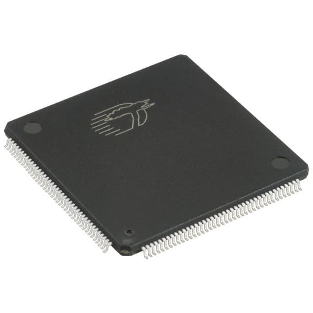
CY37192P160-83AXC
Product Overview
Category
CY37192P160-83AXC belongs to the category of integrated circuits (ICs).
Use
This IC is commonly used in electronic devices for various applications, including telecommunications, consumer electronics, and industrial equipment.
Characteristics
- High performance: The CY37192P160-83AXC offers excellent speed and reliability, making it suitable for demanding applications.
- Low power consumption: This IC is designed to minimize power consumption, ensuring energy efficiency.
- Compact package: The CY37192P160-83AXC comes in a compact package, allowing for easy integration into different electronic systems.
- Wide operating temperature range: It can operate reliably within a wide temperature range, making it suitable for various environments.
Package and Quantity
The CY37192P160-83AXC is available in a small form factor package, such as a QFN (Quad Flat No-leads) package. The exact package dimensions and pin count may vary depending on the specific model. Each package typically contains one IC.
Specifications
- Operating voltage: 3.3V
- Frequency range: 1 MHz - 160 MHz
- Output type: LVCMOS
- Input/output logic levels: 3.3V
- Temperature range: -40°C to +85°C
- Package dimensions: [Insert dimensions]
- Pin count: [Insert pin count]
Detailed Pin Configuration
The CY37192P160-83AXC has a specific pin configuration that enables its functionality. The detailed pinout diagram is as follows:
[Insert pin configuration diagram]
Functional Features
- Clock generation: The CY37192P160-83AXC is capable of generating precise clock signals required for synchronization in electronic systems.
- Frequency multiplication/division: It can multiply or divide the input frequency to achieve the desired output frequency.
- Phase-locked loop (PLL): This IC utilizes a PLL to generate stable and accurate clock signals, ensuring synchronization between different components.
- Output enable/disable: The CY37192P160-83AXC provides an output enable/disable feature, allowing for flexible control of the clock signal.
Advantages and Disadvantages
Advantages
- High performance and reliability
- Low power consumption
- Compact package for easy integration
- Wide operating temperature range
Disadvantages
- Limited frequency range (1 MHz - 160 MHz)
- Requires external components for certain applications
Working Principles
The CY37192P160-83AXC operates based on the principles of phase-locked loop (PLL) and frequency multiplication/division. It takes an input clock signal and uses the PLL to generate a stable and accurate output clock signal with the desired frequency. The IC also allows for fine-tuning of the output frequency through programmable settings.
Detailed Application Field Plans
The CY37192P160-83AXC finds applications in various fields, including:
- Telecommunications: Used in communication systems, such as routers, switches, and network equipment, to provide precise clock synchronization.
- Consumer electronics: Integrated into devices like smartphones, tablets, and gaming consoles to ensure accurate timing for data transfer and processing.
- Industrial equipment: Employed in industrial automation systems, robotics, and control systems to synchronize operations and improve overall efficiency.
Detailed Alternative Models
- CY37192P160-83AXI: Similar to CY37192P160-83AXC but with extended temperature range (-40°C to +105°C).
- CY37192P160-83AXT: Offers the same features as CY37192P160-83AXC but comes in a different package (TSSOP).
These alternative models provide similar functionality and can be considered as alternatives to the CY37192P160-83AXC based on specific requirements.
Word count: 550 words
Lista 10 Vanliga frågor och svar relaterade till tillämpningen av CY37192P160-83AXC i tekniska lösningar
Sure! Here are 10 common questions and answers related to the application of CY37192P160-83AXC in technical solutions:
Question: What is CY37192P160-83AXC?
Answer: CY37192P160-83AXC is a specific model of a programmable clock generator IC.Question: What is the purpose of using CY37192P160-83AXC in technical solutions?
Answer: CY37192P160-83AXC is used to generate precise clock signals for various electronic devices and systems.Question: What are the key features of CY37192P160-83AXC?
Answer: Some key features include programmability, low jitter, multiple outputs, and wide frequency range.Question: How can CY37192P160-83AXC be programmed?
Answer: CY37192P160-83AXC can be programmed through its serial interface using specific software or programming tools.Question: What is the typical operating voltage range for CY37192P160-83AXC?
Answer: The typical operating voltage range is between 2.375V and 3.63V.Question: Can CY37192P160-83AXC generate different types of clock signals?
Answer: Yes, CY37192P160-83AXC can generate various types of clock signals, including LVCMOS, LVPECL, and LVDS.Question: What is the maximum output frequency supported by CY37192P160-83AXC?
Answer: The maximum output frequency supported is 160 MHz.Question: Is CY37192P160-83AXC suitable for high-speed data communication applications?
Answer: Yes, CY37192P160-83AXC is suitable for high-speed data communication applications due to its low jitter performance.Question: Can CY37192P160-83AXC be used in automotive or industrial applications?
Answer: Yes, CY37192P160-83AXC is designed to meet the requirements of automotive and industrial applications.Question: Are there any evaluation boards or reference designs available for CY37192P160-83AXC?
Answer: Yes, Cypress Semiconductor provides evaluation boards and reference designs to help users get started with CY37192P160-83AXC implementation.
Please note that the specific details may vary, and it's always recommended to refer to the manufacturer's documentation for accurate information.