

CY37128VP100-83AXI
Product Overview
Category
CY37128VP100-83AXI belongs to the category of programmable logic devices (PLDs).
Use
This product is primarily used for digital circuit design and implementation. It provides a flexible and customizable solution for various applications.
Characteristics
- High-performance programmable logic device
- Advanced architecture for efficient circuit implementation
- Wide range of input/output options
- Configurable memory elements for storing data
- Support for complex logic functions
- User-friendly programming interface
Package
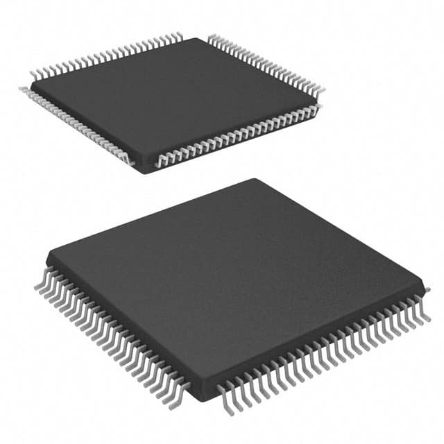
CY37128VP100-83AXI is available in a compact and durable package, ensuring easy handling and protection during transportation and installation.
Essence
The essence of CY37128VP100-83AXI lies in its ability to provide designers with a versatile platform to implement complex digital circuits efficiently.
Packaging/Quantity
This product is typically packaged in trays or tubes, with each package containing a specific quantity of CY37128VP100-83AXI devices. The exact quantity may vary depending on the supplier.
Specifications
- Device type: Programmable Logic Device (PLD)
- Family: CY37000
- Logic cells: 128 macrocells
- Speed grade: 100 MHz
- Package type: AXI
- Operating voltage: 3.3V
- I/O standards: LVTTL, LVCMOS, SSTL, HSTL, LVDS, etc.
- Temperature range: -40°C to +85°C
Detailed Pin Configuration
The pin configuration of CY37128VP100-83AXI is as follows:
- VCCIO
- GND
- TCK
- TMS
- TDI
- TDO
- VCC
- GND
- IO0
- IO1
- IO2
- IO3
- IO4
- IO5
- IO6
- IO7
- IO8
- IO9
- IO10
- IO11
- IO12
- IO13
- IO14
- IO15
- IO16
- IO17
- IO18
- IO19
- IO20
- IO21
- IO22
- IO23
- IO24
- IO25
- IO26
- IO27
- IO28
- IO29
- IO30
- IO31
Functional Features
- High-speed and efficient circuit implementation
- Configurable I/O standards for compatibility with various devices
- Flexible memory elements for data storage
- Support for complex logic functions and arithmetic operations
- User-friendly programming interface for easy configuration
Advantages and Disadvantages
Advantages
- Versatile and customizable solution for digital circuit design
- High-performance architecture for efficient implementation
- Wide range of I/O options for compatibility
- Support for complex logic functions and arithmetic operations
- User-friendly programming interface for ease of use
Disadvantages
- Limited number of logic cells compared to some other PLD models
- Higher power consumption compared to low-power alternatives
Working Principles
CY37128VP100-83AXI operates based on the principles of programmable logic devices. It consists of configurable logic blocks, input/output blocks, and interconnect resources. The device can be programmed using a hardware description language (HDL) or a graphical user interface (GUI). Once programmed, the device implements the desired digital circuit by configuring its internal resources.
Detailed Application Field Plans
CY37128VP100-83AXI finds applications in various fields, including but not limited to: - Industrial automation - Telecommunications - Automotive electronics - Consumer electronics - Medical devices - Aerospace and defense
Detailed and Complete Alternative Models
Some alternative models to CY37128VP100-83AXI include: - CY37000 series: Offers a range of options with varying logic cell counts and speed grades. - Xilinx Spartan series: Provides similar functionality with different architecture and features. - Altera MAX series: Offers programmable logic devices with different capabilities and package options.
These alternative models can be considered based on specific project requirements and design constraints.
Word count: 529 words
Lista 10 Vanliga frågor och svar relaterade till tillämpningen av CY37128VP100-83AXI i tekniska lösningar
Sure! Here are 10 common questions and answers related to the application of CY37128VP100-83AXI in technical solutions:
Question: What is the maximum operating frequency of CY37128VP100-83AXI?
Answer: The maximum operating frequency of CY37128VP100-83AXI is 100 MHz.Question: What is the voltage supply range for CY37128VP100-83AXI?
Answer: CY37128VP100-83AXI operates with a voltage supply range of 3.0V to 3.6V.Question: Can CY37128VP100-83AXI be used in industrial applications?
Answer: Yes, CY37128VP100-83AXI is suitable for industrial applications due to its robust design and wide temperature range support.Question: Does CY37128VP100-83AXI support JTAG programming?
Answer: Yes, CY37128VP100-83AXI supports JTAG programming for easy configuration and debugging.Question: What is the I/O count of CY37128VP100-83AXI?
Answer: CY37128VP100-83AXI has a total of 128 I/O pins.Question: Can CY37128VP100-83AXI interface with external memory devices?
Answer: Yes, CY37128VP100-83AXI supports various memory interfaces such as SRAM, SDRAM, and Flash.Question: Is CY37128VP100-83AXI compatible with other FPGA development tools?
Answer: Yes, CY37128VP100-83AXI is compatible with popular FPGA development tools like Xilinx ISE and Vivado.Question: What is the power consumption of CY37128VP100-83AXI?
Answer: The power consumption of CY37128VP100-83AXI depends on the specific configuration and usage, but it is designed to be power-efficient.Question: Can CY37128VP100-83AXI be used in low-power applications?
Answer: Yes, CY37128VP100-83AXI offers power-saving features like clock gating and dynamic power management, making it suitable for low-power applications.Question: Are there any application examples or reference designs available for CY37128VP100-83AXI?
Answer: Yes, Cypress provides application notes and reference designs that showcase the use of CY37128VP100-83AXI in various technical solutions. These resources can be found on their official website.