

CY2309SI-1H
Overview
Product Category
The CY2309SI-1H belongs to the category of integrated circuits (ICs) and specifically falls under the clock/timing - clock generators, PLLs, frequency synthesizers.
Use
The CY2309SI-1H is primarily used for generating clock signals in electronic devices. It provides precise timing signals that synchronize various components within a system.
Characteristics
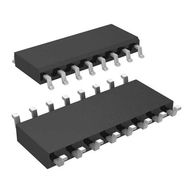
- Package: The CY2309SI-1H is available in a small outline integrated circuit (SOIC) package.
- Essence: This IC is designed to generate stable and accurate clock signals.
- Packaging/Quantity: The CY2309SI-1H is typically packaged in reels or tubes, with a quantity of 250 units per reel/tube.
Specifications
The specifications of the CY2309SI-1H include:
- Frequency Range: 1 MHz to 200 MHz
- Supply Voltage: 2.7 V to 5.5 V
- Output Format: CMOS
- Operating Temperature Range: -40°C to +85°C
- Power Dissipation: 20 mW (typical)
Pin Configuration
The CY2309SI-1H features a total of 8 pins, each serving a specific function. The pin configuration is as follows:
- VDD: Power supply voltage input
- GND: Ground reference
- XIN: Crystal oscillator input
- XOUT: Crystal oscillator output
- OE: Output enable control
- CLK_OUT: Clock signal output
- NC: No connection
- VDD: Power supply voltage input
Functional Features
The CY2309SI-1H offers several functional features, including:
- Wide frequency range selection
- Low power consumption
- High accuracy and stability
- Output enable control for easy integration into systems
- Crystal oscillator input for precise timing
Advantages and Disadvantages
Advantages
- Wide frequency range allows for versatile applications
- Low power consumption helps conserve energy
- High accuracy ensures reliable timing signals
- Output enable control offers flexibility in system integration
Disadvantages
- Limited to CMOS output format, may not be compatible with all systems
- Requires an external crystal oscillator for operation
Working Principles
The CY2309SI-1H operates based on the principles of phase-locked loop (PLL) technology. It uses a crystal oscillator as a reference to generate a stable clock signal. The PLL circuitry within the IC compares the feedback signal with the reference signal and adjusts the output frequency accordingly.
Detailed Application Field Plans
The CY2309SI-1H finds application in various electronic devices that require accurate timing signals. Some specific application fields include:
- Communication Systems: Used in network routers, switches, and modems to synchronize data transmission.
- Consumer Electronics: Integrated into televisions, DVD players, and audio systems for precise timing control.
- Automotive Electronics: Utilized in car navigation systems, infotainment units, and engine control modules for synchronized operations.
- Industrial Automation: Incorporated into programmable logic controllers (PLCs), robotics, and factory automation systems for precise timing coordination.
Detailed and Complete Alternative Models
- CY2309SXI-1H: Similar to CY2309SI-1H, but available in a small outline transistor (SOT) package.
- CY2309ZXI-1H: Offers extended temperature range (-40°C to +125°C) compared to CY2309SI-1H.
- CY2309ZC-1H: Provides additional features such as spread spectrum clocking (SSC) for reduced electromagnetic interference (EMI).
These alternative models offer similar functionality to the CY2309SI-1H but may differ in package type, temperature range, or additional features.
In conclusion, the CY2309SI-1H is a versatile clock generator IC that provides accurate and stable timing signals. Its wide frequency range, low power consumption, and output enable control make it suitable for various applications in communication systems, consumer electronics, automotive electronics, and industrial automation.
Lista 10 Vanliga frågor och svar relaterade till tillämpningen av CY2309SI-1H i tekniska lösningar
Question: What is the CY2309SI-1H?
Answer: The CY2309SI-1H is a clock generator IC that provides multiple clock outputs for various technical solutions.Question: What is the operating voltage range of the CY2309SI-1H?
Answer: The CY2309SI-1H operates within a voltage range of 2.7V to 5.5V.Question: How many clock outputs does the CY2309SI-1H provide?
Answer: The CY2309SI-1H provides nine clock outputs, including one differential output.Question: What is the maximum frequency supported by the CY2309SI-1H?
Answer: The CY2309SI-1H supports a maximum frequency of 200 MHz.Question: Can the CY2309SI-1H generate different output frequencies simultaneously?
Answer: Yes, the CY2309SI-1H can generate different output frequencies simultaneously based on its configurable PLL and dividers.Question: Does the CY2309SI-1H support spread spectrum clocking (SSC)?
Answer: No, the CY2309SI-1H does not support spread spectrum clocking.Question: What is the power supply current consumption of the CY2309SI-1H?
Answer: The power supply current consumption of the CY2309SI-1H is typically around 20 mA.Question: Is the CY2309SI-1H compatible with both CMOS and LVCMOS logic levels?
Answer: Yes, the CY2309SI-1H is compatible with both CMOS (3.3V) and LVCMOS (2.5V, 3.3V) logic levels.Question: Can the CY2309SI-1H be used in automotive applications?
Answer: No, the CY2309SI-1H is not specifically designed for automotive applications and may not meet the required standards.Question: What package options are available for the CY2309SI-1H?
Answer: The CY2309SI-1H is available in a 16-pin SOIC (Small Outline Integrated Circuit) package.