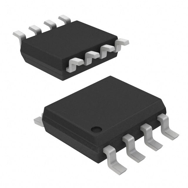
CY22801FXI
Product Overview
Category
The CY22801FXI belongs to the category of programmable clock generators.
Use
It is primarily used for generating clock signals in electronic devices and systems.
Characteristics
- Programmable clock frequency
- Flexible output options
- Low power consumption
- Wide operating voltage range
Package
The CY22801FXI comes in a compact surface-mount package.
Essence
The essence of the CY22801FXI lies in its ability to generate precise clock signals with customizable frequencies.
Packaging/Quantity
The CY22801FXI is typically packaged in reels and is available in quantities of 1000 units per reel.
Specifications
- Input voltage: 2.7V to 3.6V
- Output frequency range: 1MHz to 200MHz
- Output types: LVCMOS, LVPECL, LVDS, HCSL
- Programmable features: frequency, output type, spread spectrum modulation
Detailed Pin Configuration
The CY22801FXI has a total of 16 pins. The pin configuration is as follows:
- VDD - Power supply input
- GND - Ground
- XIN - Crystal oscillator input
- XOUT - Crystal oscillator output
- VDDPLL - PLL power supply input
- GNDPLL - PLL ground
- VDDO - Output power supply input
- GNDIO - Output ground
- OE - Output enable control
- S0 - Frequency selection input
- S1 - Frequency selection input
- S2 - Frequency selection input
- S3 - Frequency selection input
- CLKOUT - Clock output
- NC - No connection
- NC - No connection
Functional Features
- Programmable frequency selection through input pins
- Multiple output types for compatibility with different systems
- Spread spectrum modulation capability for reduced electromagnetic interference
Advantages and Disadvantages
Advantages
- High flexibility in generating clock signals
- Low power consumption
- Wide operating voltage range allows for use in various applications
Disadvantages
- Limited output frequency range compared to some other models
- Requires external crystal oscillator for operation
Working Principles
The CY22801FXI utilizes a phase-locked loop (PLL) to generate clock signals. The PLL locks onto an input reference frequency and generates an output clock signal with a programmable frequency. The output frequency is determined by the combination of frequency selection inputs.
Detailed Application Field Plans
The CY22801FXI can be used in various electronic devices and systems that require precise clock signals. Some potential application fields include:
- Communication systems
- Computer peripherals
- Industrial automation
- Consumer electronics
- Automotive electronics
Detailed and Complete Alternative Models
- CY22800FXI - Similar to CY22801FXI, but with a wider output frequency range.
- CY22802FXI - Similar to CY22801FXI, but with additional features such as integrated voltage regulators.
- CY22803FXI - Similar to CY22801FXI, but optimized for low-power applications.
These alternative models provide options with different specifications and features to suit specific requirements.
Word count: 430 words
Lista 10 Vanliga frågor och svar relaterade till tillämpningen av CY22801FXI i tekniska lösningar
Sure! Here are 10 common questions and answers related to the application of CY22801FXI in technical solutions:
Q: What is CY22801FXI? A: CY22801FXI is a programmable spread spectrum clock generator (SSCG) integrated circuit (IC) designed for reducing electromagnetic interference (EMI) in electronic systems.
Q: How does CY22801FXI help in reducing EMI? A: CY22801FXI uses spread spectrum techniques to modulate the output clock frequency, spreading the energy across a wider frequency range and reducing peak emissions, thereby minimizing EMI.
Q: What are the key features of CY22801FXI? A: Some key features of CY22801FXI include programmable spread spectrum modulation, wide frequency range support, low power consumption, and easy integration into various system designs.
Q: In which applications can CY22801FXI be used? A: CY22801FXI can be used in a wide range of applications such as computer motherboards, graphics cards, networking equipment, industrial control systems, and consumer electronics.
Q: How do I program CY22801FXI? A: CY22801FXI can be programmed using an external EEPROM or through an I2C interface, allowing users to configure the desired spread spectrum modulation parameters.
Q: Can CY22801FXI generate multiple output clocks? A: Yes, CY22801FXI supports up to four independent output clocks, each with its own programmable spread spectrum modulation settings.
Q: What is the operating voltage range of CY22801FXI? A: CY22801FXI operates from a supply voltage range of 2.7V to 3.6V, making it compatible with a wide range of power supply systems.
Q: Does CY22801FXI support frequency margining? A: Yes, CY22801FXI supports frequency margining, allowing users to adjust the output clock frequency within a specified range for testing or system optimization purposes.
Q: Can CY22801FXI be used in battery-powered devices? A: Yes, CY22801FXI's low power consumption makes it suitable for use in battery-powered devices where EMI reduction is required.
Q: Is CY22801FXI compliant with industry standards? A: Yes, CY22801FXI is compliant with various industry standards such as PCI Express (PCIe), Universal Serial Bus (USB), and Serial ATA (SATA), ensuring compatibility with modern electronic systems.
Please note that these answers are general and may vary depending on specific application requirements.


