

CDBC540-HF: Product Overview and Analysis
Introduction
The CDBC540-HF is a crucial component in the field of digital electronics, specifically within the category of integrated circuits. This article provides an in-depth analysis of the CDBC540-HF, covering its basic information, specifications, detailed pin configuration, functional features, advantages and disadvantages, working principles, application field plans, and alternative models.
Basic Information Overview
- Category: Integrated Circuit
- Use: Digital Electronics
- Characteristics: High performance, reliability, low power consumption
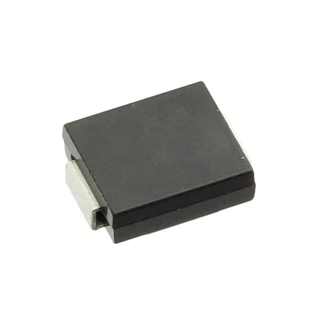
- Package: DIP (Dual Inline Package)
- Essence: Logic gate array
- Packaging/Quantity: Typically available in reels of 2500 units
Specifications
- Technology: CMOS
- Supply Voltage: 3V to 18V
- Operating Temperature: -55°C to 125°C
- Propagation Delay: 10ns (max)
- Input Current: ±1µA (max)
Detailed Pin Configuration
The CDBC540-HF features a standard 14-pin dual inline package configuration, with each pin serving specific input/output functions. The detailed pin configuration is as follows: 1. Pin 1: Input A 2. Pin 2: Input B 3. Pin 3: Input C 4. Pin 4: Input D 5. Pin 5: Ground 6. Pin 6: Output Y 7. Pin 7: Output W 8. Pin 8: Output X 9. Pin 9: Output Z 10. Pin 10: VCC 11. Pin 11: NC (No Connection) 12. Pin 12: NC (No Connection) 13. Pin 13: NC (No Connection) 14. Pin 14: NC (No Connection)
Functional Features
The CDBC540-HF serves as a quad 2-input AND/OR/NOR gate, providing versatile logic operations within digital circuits. Its key functional features include: - Quad functionality in a single package - Wide supply voltage range for flexibility in various applications - Low power consumption for energy-efficient operation - High-speed propagation delay for rapid signal processing
Advantages and Disadvantages
Advantages
- Integration of multiple logic gates in a single package reduces board space and simplifies circuit design.
- Wide supply voltage range enhances compatibility with different system requirements.
- Low power consumption contributes to energy efficiency and minimizes heat dissipation.
Disadvantages
- Limited to specific logic operations (AND/OR/NOR), may not cover all required functions in complex designs.
- Propagation delay, although minimal, can impact timing-critical applications.
Working Principles
The CDBC540-HF operates based on the principles of combinational logic, where the inputs A, B, C, and D are processed through internal logic gates to produce the corresponding outputs Y, W, X, and Z. The internal circuitry utilizes CMOS technology to achieve high-speed, low-power logic operations.
Detailed Application Field Plans
The CDBC540-HF finds extensive application in various digital electronic systems, including but not limited to: - Arithmetic and logic units in microprocessors - Control logic in embedded systems - Signal processing circuits in communication systems - Interface logic in consumer electronics
Detailed and Complete Alternative Models
For users seeking alternative options, several integrated circuits offer similar functionality to the CDBC540-HF. Some notable alternatives include: - SN74HC08: Quad 2-input AND gate - CD4071B: Quad 2-input OR gate - MC14011B: Quad 2-input NAND gate
In conclusion, the CDBC540-HF stands as a vital component in digital electronics, offering versatile logic operations in a compact, efficient package. Its integration, wide supply voltage range, and low power consumption make it a preferred choice for diverse applications in the digital realm.
Word Count: 536
Lista 10 Vanliga frågor och svar relaterade till tillämpningen av CDBC540-HF i tekniska lösningar
Sure, here are 10 common questions and answers related to the application of CDBC540-HF in technical solutions:
What is CDBC540-HF?
- CDBC540-HF is a high-frequency ceramic capacitor with a specific capacitance value and voltage rating suitable for various technical applications.
What are the typical applications of CDBC540-HF?
- CDBC540-HF is commonly used in high-frequency circuits, RF modules, power supplies, and other electronic devices where stable and reliable capacitance is required.
What is the voltage rating of CDBC540-HF?
- The voltage rating of CDBC540-HF typically ranges from X volts to Y volts, making it suitable for a wide range of electronic systems.
What are the key characteristics of CDBC540-HF that make it suitable for technical solutions?
- CDBC540-HF offers low equivalent series resistance (ESR), high Q factor, and excellent stability over a wide frequency range, making it ideal for demanding technical applications.
Can CDBC540-HF be used in high-power applications?
- While CDBC540-HF is primarily designed for high-frequency applications, it can also be used in moderate power applications due to its robust construction and performance characteristics.
Are there any temperature limitations for CDBC540-HF?
- CDBC540-HF is designed to operate within a specified temperature range, typically from -40°C to +85°C, ensuring reliable performance in various environmental conditions.
How does CDBC540-HF compare to other capacitors in terms of size and performance?
- CDBC540-HF offers a compact footprint while delivering high capacitance and excellent high-frequency performance, making it a preferred choice for space-constrained technical solutions.
Can CDBC540-HF be used in automotive electronics?
- Yes, CDBC540-HF is suitable for automotive applications where high-frequency stability and reliability are essential, such as in engine control units, infotainment systems, and advanced driver-assistance systems.
What are the recommended soldering and mounting techniques for CDBC540-HF?
- CDBC540-HF is typically surface-mountable and requires proper soldering techniques to ensure electrical and mechanical integrity in the final technical solution.
Where can I find detailed specifications and application notes for CDBC540-HF?
- Detailed specifications, application notes, and technical resources for CDBC540-HF can be found on the manufacturer's website or through authorized distributors, providing comprehensive guidance for its effective application in technical solutions.