

WM8533ECSN/R
Product Overview
Category: Integrated Circuit (IC)
Use: The WM8533ECSN/R is a versatile integrated circuit primarily used for audio processing and amplification in various electronic devices.
Characteristics: - High-quality audio signal processing - Low power consumption - Compact size - Wide operating voltage range - Excellent noise performance
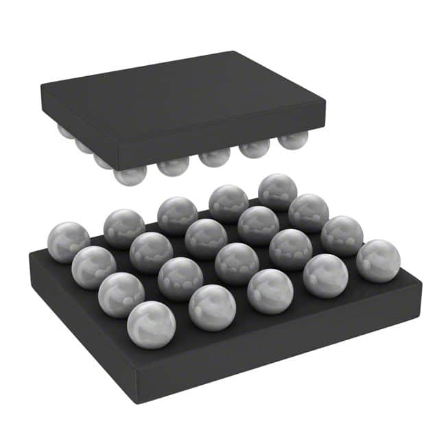
Package: The WM8533ECSN/R is available in a small outline package (SOP) with a specified pin configuration.
Essence: This IC is designed to enhance audio quality and provide efficient audio signal processing capabilities in electronic devices.
Packaging/Quantity: The WM8533ECSN/R is typically packaged in reels or tubes, with a quantity of 2500 units per reel/tube.
Specifications
The WM8533ECSN/R offers the following specifications:
- Supply Voltage Range: 2.7V to 5.5V
- Operating Temperature Range: -40°C to +85°C
- Total Harmonic Distortion (THD): <0.01%
- Signal-to-Noise Ratio (SNR): >90dB
- Output Power: Up to 1W
- Package Type: SOP-16
Pin Configuration
The detailed pin configuration of the WM8533ECSN/R is as follows:
| Pin Number | Pin Name | Function | |------------|----------|----------| | 1 | VDD | Power Supply (Positive) | | 2 | GND | Ground | | 3 | INL | Audio Input (Left Channel) | | 4 | INR | Audio Input (Right Channel) | | 5 | BYPASS | Bypass Mode Control | | 6 | MUTE | Mute Control | | 7 | VREF | Reference Voltage | | 8 | OUTL | Audio Output (Left Channel) | | 9 | OUTR | Audio Output (Right Channel) | | 10 | AGND | Analog Ground | | 11 | NC | No Connection | | 12 | NC | No Connection | | 13 | NC | No Connection | | 14 | NC | No Connection | | 15 | NC | No Connection | | 16 | VDD | Power Supply (Positive) |
Functional Features
The WM8533ECSN/R offers the following functional features:
- High-fidelity audio signal processing
- Built-in amplification for improved audio output
- Bypass mode for direct audio signal routing
- Mute control for audio output suppression
- Low power consumption for energy-efficient operation
- Wide operating voltage range for compatibility with various systems
Advantages and Disadvantages
Advantages: - High-quality audio processing and amplification - Compact size allows for integration into small electronic devices - Excellent noise performance ensures clear audio output - Versatile functionality suitable for a wide range of applications
Disadvantages: - Limited output power compared to dedicated audio amplifiers - May require additional external components for certain applications
Working Principles
The WM8533ECSN/R operates by receiving audio input signals through the INL and INR pins. These signals are then processed and amplified internally before being output through the OUTL and OUTR pins. The IC also provides options for bypassing the internal processing and muting the audio output when necessary.
Detailed Application Field Plans
The WM8533ECSN/R is widely used in various electronic devices that require audio processing and amplification, including but not limited to: - Portable audio players - Mobile phones - Tablets and laptops - Home theater systems - Car audio systems
Detailed and Complete Alternative Models
- WM8534ECSN/R: Similar to the WM8533ECSN/R with enhanced power output capabilities.
- WM8535ECSN/R: A higher-end version of the WM8533ECSN/R with advanced audio processing features.
- WM8536ECSN/R: A lower-cost alternative with basic audio amplification functionality.
These alternative models offer similar functionality and can be considered based on specific requirements and budget constraints.
Word count: 533 words
Lista 10 Vanliga frågor och svar relaterade till tillämpningen av WM8533ECSN/R i tekniska lösningar
What is the maximum input voltage for WM8533ECSN/R?
- The maximum input voltage for WM8533ECSN/R is 5.5V.What is the typical output current capability of WM8533ECSN/R?
- The typical output current capability of WM8533ECSN/R is 300mA.Can WM8533ECSN/R be used in battery-powered applications?
- Yes, WM8533ECSN/R can be used in battery-powered applications due to its low quiescent current.What is the typical dropout voltage of WM8533ECSN/R?
- The typical dropout voltage of WM8533ECSN/R is 240mV at 150mA load.Is WM8533ECSN/R suitable for use in automotive applications?
- Yes, WM8533ECSN/R is suitable for use in automotive applications due to its wide input voltage range and robust design.Does WM8533ECSN/R have built-in thermal shutdown protection?
- Yes, WM8533ECSN/R features built-in thermal shutdown protection to prevent overheating.What is the operating temperature range of WM8533ECSN/R?
- The operating temperature range of WM8533ECSN/R is -40°C to 125°C.Can WM8533ECSN/R be used in space-constrained designs?
- Yes, WM8533ECSN/R is available in a small footprint package, making it suitable for space-constrained designs.Does WM8533ECSN/R require external compensation components?
- No, WM8533ECSN/R is internally compensated and does not require external compensation components.Is WM8533ECSN/R RoHS compliant?
- Yes, WM8533ECSN/R is RoHS compliant, making it suitable for environmentally conscious designs.