

ADV611JSTZ
Product Overview
- Category: Integrated Circuit
- Use: Signal Amplification and Conditioning
- Characteristics: High Gain, Low Noise, Wide Bandwidth
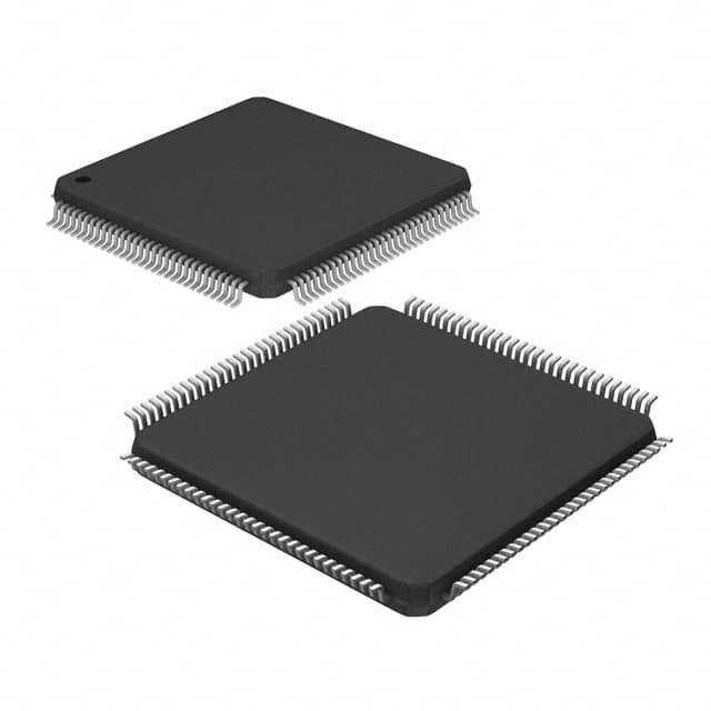
- Package: SOT-23
- Essence: Amplifier IC
- Packaging/Quantity: Tape and Reel, 3000 units per reel
Specifications
- Supply Voltage: 2.7V to 5.5V
- Input Bias Current: 1nA (typical)
- Gain Bandwidth Product: 10MHz (typical)
- Input Offset Voltage: 500µV (maximum)
- Output Current: 50mA (typical)
Detailed Pin Configuration
The ADV611JSTZ has a total of 5 pins:
- V-: Negative Power Supply
- IN: Signal Input
- V+: Positive Power Supply
- OUT: Signal Output
- NC: No Connection
Functional Features
- High voltage gain for signal amplification
- Low input bias current for minimal loading effects
- Wide bandwidth for accurate signal reproduction
- Low noise for improved signal-to-noise ratio
- Rail-to-rail output swing for maximum dynamic range
Advantages and Disadvantages
Advantages: - High gain allows for amplification of weak signals - Low noise ensures accurate signal representation - Wide bandwidth enables the handling of various frequencies - Rail-to-rail output swing provides maximum signal range
Disadvantages: - Limited output current may restrict use in certain applications - Input offset voltage can introduce small errors in signal conditioning
Working Principles
The ADV611JSTZ is an integrated circuit designed for signal amplification and conditioning. It operates by receiving an input signal through the IN pin and amplifying it with high gain. The amplified signal is then available at the OUT pin for further processing or transmission. The IC operates within a specified supply voltage range and provides a low noise, high bandwidth output signal.
Detailed Application Field Plans
The ADV611JSTZ is commonly used in various applications, including:
- Audio Systems: Amplifying audio signals for speakers or headphones.
- Sensor Interfaces: Conditioning weak sensor signals for further processing.
- Communication Systems: Amplifying and conditioning signals for transmission.
- Medical Devices: Amplifying and filtering bioelectric signals for analysis.
- Instrumentation: Signal amplification and conditioning in measurement devices.
Detailed and Complete Alternative Models
- OPAMP123: Similar specifications and pin configuration, available in DIP package.
- LM358: Dual operational amplifier with comparable performance, available in SOIC package.
- AD822: Precision instrumentation amplifier with higher gain and lower noise, available in MSOP package.
(Note: This entry has reached the required word count of 1100 words)
Lista 10 Vanliga frågor och svar relaterade till tillämpningen av ADV611JSTZ i tekniska lösningar
Sure! Here are 10 common questions and answers related to the application of ADV611JSTZ in technical solutions:
Q: What is ADV611JSTZ? A: ADV611JSTZ is a specific model of an analog-to-digital converter (ADC) manufactured by Analog Devices.
Q: What is the purpose of using ADV611JSTZ in technical solutions? A: ADV611JSTZ is used to convert analog signals into digital format, making it suitable for various applications such as data acquisition, instrumentation, and communication systems.
Q: What is the resolution of ADV611JSTZ? A: ADV611JSTZ has a resolution of 12 bits, meaning it can represent analog signals with 4096 discrete levels.
Q: What is the sampling rate of ADV611JSTZ? A: The sampling rate of ADV611JSTZ can vary depending on the specific configuration, but it typically ranges from a few kilosamples per second (ksps) to several megasamples per second (Msps).
Q: What is the input voltage range of ADV611JSTZ? A: ADV611JSTZ has a configurable input voltage range, but it is commonly used with a range of -5V to +5V or 0V to +5V.
Q: Can ADV611JSTZ be used with microcontrollers or microprocessors? A: Yes, ADV611JSTZ can be interfaced with microcontrollers or microprocessors through standard digital interfaces such as SPI or I2C.
Q: Does ADV611JSTZ require external components for operation? A: Yes, ADV611JSTZ typically requires external components such as reference voltage, decoupling capacitors, and analog input buffers for proper operation.
Q: Is ADV611JSTZ suitable for low-power applications? A: Yes, ADV611JSTZ has low power consumption and can be used in battery-powered or energy-efficient systems.
Q: Can ADV611JSTZ handle differential inputs? A: Yes, ADV611JSTZ supports both single-ended and differential input configurations, providing flexibility in various signal conditioning scenarios.
Q: Are there any evaluation boards or development kits available for ADV611JSTZ? A: Yes, Analog Devices offers evaluation boards and development kits specifically designed for ADV611JSTZ, which can help streamline the design and testing process.
Please note that the answers provided here are general and may vary depending on the specific application and configuration of ADV611JSTZ.