

ADN2816ACPZ-RL7
Overview
Category
ADN2816ACPZ-RL7 belongs to the category of integrated circuits (ICs).
Use
This product is commonly used in electronic devices for signal processing and communication applications.
Characteristics
- High-performance integrated circuit
- Designed for signal processing and communication
- Compact size and low power consumption
Package
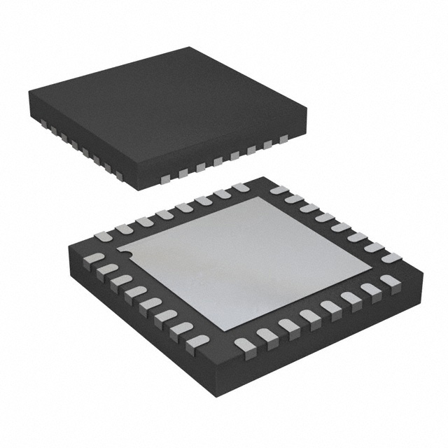
ADN2816ACPZ-RL7 is available in a small form factor package, specifically the LFCSP (Lead Frame Chip Scale Package).
Essence
The essence of ADN2816ACPZ-RL7 lies in its ability to process signals efficiently and accurately, enhancing communication performance.
Packaging/Quantity
This product is typically packaged in reels or trays, with a quantity of 2500 units per reel.
Specifications and Parameters
- Supply Voltage: 3.3V
- Operating Temperature Range: -40°C to +85°C
- Data Rate: Up to 2.5 Gbps
- Power Consumption: 150mW
- Input Impedance: 50Ω
Pin Configuration
The pin configuration of ADN2816ACPZ-RL7 is as follows:
- VCC
- GND
- NC
- NC
- NC
- NC
- NC
- NC
- NC
- NC
- NC
- NC
- NC
- NC
- NC
- NC
Functional Characteristics
ADN2816ACPZ-RL7 offers the following functional characteristics:
- Signal amplification
- Signal filtering
- Clock recovery
- Data retiming
Advantages and Disadvantages
Advantages
- High-performance signal processing
- Compact size
- Low power consumption
Disadvantages
- Limited data rate (up to 2.5 Gbps)
- Specific use case in signal processing and communication applications
Applicable Range of Products
ADN2816ACPZ-RL7 is applicable in various electronic devices, including: - Optical transceivers - Network switches - Communication equipment
Working Principles
The working principle of ADN2816ACPZ-RL7 involves receiving input signals, amplifying and filtering them, recovering the clock signal, and retiming the data for further processing.
Detailed Application Field Plans
ADN2816ACPZ-RL7 can be used in the following application fields: 1. Fiber optic communication systems 2. Data center networking 3. Telecommunication infrastructure 4. High-speed data transmission 5. Wireless communication systems
Detailed Alternative Models
Some alternative models to ADN2816ACPZ-RL7 include: - ADN2817ACPZ-RL7 - ADN2818ACPZ-RL7 - ADN2819ACPZ-RL7 - ADN2820ACPZ-RL7 - ADN2821ACPZ-RL7
5 Common Technical Questions and Answers
Q: What is the maximum data rate supported by ADN2816ACPZ-RL7? A: The maximum data rate supported is 2.5 Gbps.
Q: What is the power consumption of this product? A: The power consumption is approximately 150mW.
Q: What is the operating temperature range for ADN2816ACPZ-RL7? A: The operating temperature range is -40°C to +85°C.
Q: What is the package type for this IC? A: ADN2816ACPZ-RL7 is available in the LFCSP package.
Q: What is the input impedance of ADN2816ACPZ-RL7? A: The input impedance is 50Ω.
This concludes the encyclopedia entry for ADN2816ACPZ-RL7, a high-performance integrated circuit used in signal processing and communication applications.