

ADCMP580BCPZ-RL7
Product Overview
Category
The ADCMP580BCPZ-RL7 belongs to the category of analog-to-digital converters (ADCs).
Use
This product is primarily used for converting analog signals into digital data, making it suitable for a wide range of applications in various industries.
Characteristics
- High precision: The ADCMP580BCPZ-RL7 offers exceptional accuracy in converting analog signals to digital form.
- Fast conversion speed: With its high-speed conversion capability, this ADC ensures efficient signal processing.
- Low power consumption: The device is designed to operate with minimal power consumption, making it energy-efficient.
- Small package size: The compact package allows for easy integration into different electronic systems.
- Wide operating voltage range: The ADCMP580BCPZ-RL7 can function within a broad voltage range, enhancing its versatility.
Package and Quantity
The ADCMP580BCPZ-RL7 is available in a small-sized package, typically provided in reels. The exact packaging and quantity may vary depending on the supplier.
Specifications
- Resolution: 12 bits
- Input Voltage Range: 0V to Vref
- Conversion Rate: Up to 1 MSPS (Mega Samples Per Second)
- Power Supply Voltage: 2.7V to 5.5V
- Operating Temperature Range: -40°C to +85°C
- Interface: Serial Peripheral Interface (SPI)
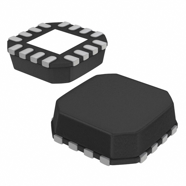
Pin Configuration
The ADCMP580BCPZ-RL7 features the following pin configuration:
- VDD: Power supply voltage input
- GND: Ground reference
- CS: Chip select input
- SCLK: Serial clock input
- SDI: Serial data input
- SDO: Serial data output
- REF: Reference voltage input
- IN: Analog input
Functional Features
- High-resolution conversion: The ADCMP580BCPZ-RL7 provides accurate conversion of analog signals into 12-bit digital data.
- Fast conversion speed: With a maximum conversion rate of 1 MSPS, this ADC ensures efficient signal processing.
- Low power consumption: The device is designed to operate with minimal power consumption, making it suitable for battery-powered applications.
- SPI interface: The Serial Peripheral Interface allows for easy integration with microcontrollers and other digital systems.
Advantages and Disadvantages
Advantages
- High precision conversion
- Fast conversion speed
- Low power consumption
- Compact package size
- Wide operating voltage range
Disadvantages
- Limited resolution compared to higher-end ADCs
- Requires an external reference voltage source
Working Principles
The ADCMP580BCPZ-RL7 operates based on the principle of successive approximation. It samples the analog input voltage and compares it to a reference voltage. By iteratively adjusting the digital code, the converter converges to a digital representation that closely matches the input voltage.
Detailed Application Field Plans
The ADCMP580BCPZ-RL7 can be used in various applications, including but not limited to: - Industrial automation - Medical equipment - Test and measurement instruments - Communication systems - Consumer electronics
Alternative Models
For those seeking alternative options, the following models are worth considering: - ADCMP581BCPZ-RL7: Similar specifications with enhanced resolution (14 bits) - ADCMP582BCPZ-RL7: Higher-speed conversion capability (up to 2 MSPS) - ADCMP583BCPZ-RL7: Lower power consumption variant
These alternatives provide flexibility in choosing the most suitable ADC for specific requirements.
In conclusion, the ADCMP580BCPZ-RL7 is a high-precision analog-to-digital converter with fast conversion speed and low power consumption. Its compact size and wide operating voltage range make it suitable for various applications. While it has some limitations in resolution and requires an external reference voltage, alternative models offer different features to cater to specific needs.
Lista 10 Vanliga frågor och svar relaterade till tillämpningen av ADCMP580BCPZ-RL7 i tekniska lösningar
What is the supply voltage range for ADCMP580BCPZ-RL7?
- The supply voltage range for ADCMP580BCPZ-RL7 is 2.7V to 5.5V.What is the typical propagation delay of ADCMP580BCPZ-RL7?
- The typical propagation delay of ADCMP580BCPZ-RL7 is 1.3ns.Can ADCMP580BCPZ-RL7 be used in high-speed communication systems?
- Yes, ADCMP580BCPZ-RL7 is suitable for high-speed communication systems due to its fast response time.What is the input common-mode voltage range for ADCMP580BCPZ-RL7?
- The input common-mode voltage range for ADCMP580BCPZ-RL7 is -0.2V to VDD+0.2V.Is ADCMP580BCPZ-RL7 compatible with TTL and CMOS logic levels?
- Yes, ADCMP580BCPZ-RL7 is compatible with both TTL and CMOS logic levels.Can ADCMP580BCPZ-RL7 be used in battery-powered applications?
- Yes, ADCMP580BCPZ-RL7's low supply voltage range makes it suitable for battery-powered applications.What is the temperature range for ADCMP580BCPZ-RL7?
- ADCMP580BCPZ-RL7 operates within a temperature range of -40°C to 125°C.Does ADCMP580BCPZ-RL7 have built-in hysteresis?
- Yes, ADCMP580BCPZ-RL7 features built-in hysteresis for improved noise immunity.Can ADCMP580BCPZ-RL7 be used in automotive applications?
- Yes, ADCMP580BCPZ-RL7 is qualified for automotive applications.What is the package type for ADCMP580BCPZ-RL7?
- ADCMP580BCPZ-RL7 is available in a lead-free, 8-lead LFCSP package.