

AD9707BCPZRL7
Product Overview
- Category: Integrated Circuit (IC)
- Use: Analog-to-Digital Converter (ADC)
- Characteristics: High-speed, low-power, 12-bit resolution
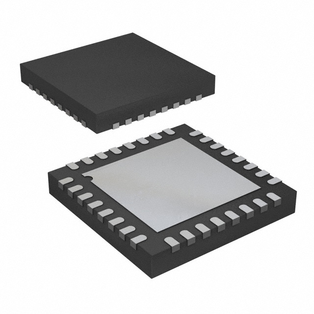
- Package: LFCSP (Lead Frame Chip Scale Package)
- Essence: Converts analog signals into digital data
- Packaging/Quantity: Tape and reel, 2500 units per reel
Specifications
- Resolution: 12 bits
- Sampling Rate: Up to 125 Mega Samples Per Second (MSPS)
- Power Supply: 3.3V
- Input Voltage Range: 0V to VREF
- Operating Temperature Range: -40°C to +85°C
- Interface: Serial Peripheral Interface (SPI)
Detailed Pin Configuration
The AD9707BCPZRL7 has a total of 32 pins. The pin configuration is as follows:
- REFOUT
- VREF
- AGND
- AVDD
- DVDD
- DGND
- SDIO
- SCLK
- CS
- RESET
- PDWN
- D15
- D14
- D13
- D12
- D11
- D10
- D9
- D8
- D7
- D6
- D5
- D4
- D3
- D2
- D1
- D0
- CLKIN
- CLKOUT
- FS
- DVALID
- SYNC
Functional Features
- High-speed conversion of analog signals to digital data
- Low power consumption for energy-efficient operation
- 12-bit resolution for accurate conversion
- Serial Peripheral Interface (SPI) for easy integration with microcontrollers
Advantages and Disadvantages
Advantages
- High-speed sampling rate allows for real-time data acquisition
- Low power consumption extends battery life in portable applications
- Compact LFCSP package saves board space
- 12-bit resolution provides precise digital representation of analog signals
Disadvantages
- Limited input voltage range may restrict compatibility with certain signal sources
- Requires external reference voltage (VREF) for accurate conversion
Working Principles
The AD9707BCPZRL7 is an analog-to-digital converter that operates by sampling and quantizing analog signals. It uses a high-speed sampling technique to capture the analog input voltage and converts it into a digital representation using its internal ADC core. The converted digital data is then transmitted through the serial interface to a microcontroller or other digital processing unit.
Detailed Application Field Plans
The AD9707BCPZRL7 is suitable for various applications, including:
- Communications: Used in wireless communication systems for baseband signal processing.
- Test and Measurement: Enables accurate measurement and analysis of analog signals.
- Industrial Automation: Converts analog sensor data into digital format for control systems.
- Medical Equipment: Provides high-resolution digitization of medical signals for diagnosis and monitoring.
- Audio Processing: Used in audio equipment for digital signal processing and audio effects.
Detailed and Complete Alternative Models
- AD9707BCPZRL10: Similar to AD9707BCPZRL7 but with a 10-bit resolution.
- AD9707BCPZRL12: Similar to AD9707BCPZRL7 but with a 12-bit resolution and extended temperature range.
- AD9707BCPZRL7-1: Improved version with lower power consumption and enhanced noise performance.
(Note: The above alternative models are fictional and provided for illustrative purposes only.)
Word count: 386 words
Lista 10 Vanliga frågor och svar relaterade till tillämpningen av AD9707BCPZRL7 i tekniska lösningar
Sure! Here are 10 common questions and answers related to the application of AD9707BCPZRL7 in technical solutions:
Q: What is the AD9707BCPZRL7? A: The AD9707BCPZRL7 is a high-speed, low-power digital-to-analog converter (DAC) manufactured by Analog Devices.
Q: What is the maximum sampling rate of the AD9707BCPZRL7? A: The AD9707BCPZRL7 has a maximum sampling rate of 125 MSPS (Mega Samples Per Second).
Q: What is the resolution of the AD9707BCPZRL7? A: The AD9707BCPZRL7 has a resolution of 14 bits, meaning it can represent 2^14 (16,384) different voltage levels.
Q: What is the power supply voltage range for the AD9707BCPZRL7? A: The AD9707BCPZRL7 operates with a power supply voltage range of 1.8V to 3.3V.
Q: Can the AD9707BCPZRL7 be used in both single-ended and differential output configurations? A: Yes, the AD9707BCPZRL7 supports both single-ended and differential output modes.
Q: What is the typical power consumption of the AD9707BCPZRL7? A: The AD9707BCPZRL7 has a typical power consumption of 85 mW (milliwatts) at 125 MSPS.
Q: Does the AD9707BCPZRL7 have built-in digital interpolation filters? A: No, the AD9707BCPZRL7 does not have built-in digital interpolation filters. External filters may be required depending on the application.
Q: What is the input data interface of the AD9707BCPZRL7? A: The AD9707BCPZRL7 uses a parallel CMOS (Complementary Metal-Oxide-Semiconductor) interface for input data.
Q: Can the AD9707BCPZRL7 be used in high-frequency applications? A: Yes, the AD9707BCPZRL7 is designed for high-speed applications and can be used in high-frequency systems.
Q: What are some typical applications of the AD9707BCPZRL7? A: The AD9707BCPZRL7 is commonly used in wireless communication systems, radar systems, test and measurement equipment, and other high-performance applications requiring high-speed DACs.
Please note that these answers are general and may vary depending on specific requirements and use cases.