

U62256ADK07LLG1
Basic Information Overview
- Category: Integrated Circuit (IC)
- Use: Memory chip
- Characteristics:
- Non-volatile
- High storage capacity
- Low power consumption
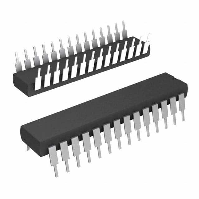
- Package: DIP (Dual In-line Package)
- Essence: Data storage and retrieval
- Packaging/Quantity: Individually packaged, quantity varies based on supplier
Specifications
- Memory Capacity: 256 kilobits (32 kilobytes)
- Organization: 32 kilobytes x 8 bits
- Supply Voltage: 2.7V to 5.5V
- Access Time: 70 ns
- Operating Temperature Range: -40°C to +85°C
- Interface: Parallel
Detailed Pin Configuration
The U62256ADK07LLG1 has a total of 28 pins. The pin configuration is as follows:
- Chip Enable (CE)
- Output Enable (OE)
- Write Enable (WE)
- Address Inputs (A0-A14)
- Data Inputs/Outputs (DQ0-DQ7)
- Power Supply (+5V)
- Ground (GND)
Functional Features
- Random access memory (RAM) functionality
- Non-volatile storage capability
- Low power consumption in standby mode
- Fast data access time
- Easy integration with microcontrollers and other ICs
Advantages
- High storage capacity for its size
- Non-volatile nature ensures data retention even during power loss
- Low power consumption extends battery life in portable devices
- Fast access time allows for quick data retrieval
- Versatile interface enables compatibility with various systems
Disadvantages
- Relatively slower access time compared to modern memory technologies
- Limited storage capacity compared to newer memory chips
- Higher cost per bit compared to larger memory chips
Working Principles
The U62256ADK07LLG1 is based on the technology of static random access memory (SRAM). It stores data using flip-flops, which retain their state as long as power is supplied. The chip uses an address bus to select specific memory locations and a data bus to read from or write to those locations. The control pins (CE, OE, WE) determine the chip's operational mode.
Detailed Application Field Plans
The U62256ADK07LLG1 can be used in various applications, including: - Embedded systems - Industrial automation - Consumer electronics - Automotive electronics - Medical devices
Detailed and Complete Alternative Models
Some alternative models that offer similar functionality to the U62256ADK07LLG1 include: - AT28C256 - Atmel - 25LC256 - Microchip Technology - M24C256 - STMicroelectronics - CY62256 - Cypress Semiconductor
Note: This list is not exhaustive, and there are other alternatives available in the market.
Word count: 314 words
Lista 10 Vanliga frågor och svar relaterade till tillämpningen av U62256ADK07LLG1 i tekniska lösningar
Question: What is U62256ADK07LLG1?
Answer: U62256ADK07LLG1 is a specific model of a 32K x 8-bit high-speed CMOS static RAM (SRAM) chip.Question: What are the key features of U62256ADK07LLG1?
Answer: Some key features of U62256ADK07LLG1 include a 32K-byte capacity, low power consumption, fast access time, and compatibility with various microcontrollers and digital systems.Question: What is the typical application of U62256ADK07LLG1?
Answer: U62256ADK07LLG1 is commonly used in applications that require temporary data storage, such as embedded systems, industrial control systems, communication equipment, and consumer electronics.Question: How does U62256ADK07LLG1 connect to a microcontroller or digital system?
Answer: U62256ADK07LLG1 connects to a microcontroller or digital system using standard parallel interface pins, typically through address, data, and control lines.Question: What is the operating voltage range for U62256ADK07LLG1?
Answer: U62256ADK07LLG1 operates within a voltage range of 4.5V to 5.5V.Question: Can U62256ADK07LLG1 be used in battery-powered devices?
Answer: Yes, U62256ADK07LLG1 has low power consumption, making it suitable for battery-powered devices where energy efficiency is crucial.Question: Does U62256ADK07LLG1 have any built-in error correction mechanisms?
Answer: No, U62256ADK07LLG1 does not have built-in error correction mechanisms. However, it can be used in conjunction with external error correction techniques if required.Question: What is the access time of U62256ADK07LLG1?
Answer: The access time of U62256ADK07LLG1 is typically around 70-120 nanoseconds, depending on the specific operating conditions.Question: Can U62256ADK07LLG1 be easily replaced or upgraded in an existing system?
Answer: Yes, U62256ADK07LLG1 has a standard pinout and is compatible with other similar SRAM chips, making it relatively easy to replace or upgrade in an existing system.Question: Are there any specific precautions to consider when using U62256ADK07LLG1?
Answer: It is important to handle U62256ADK07LLG1 according to proper electrostatic discharge (ESD) precautions to prevent damage. Additionally, the datasheet provided by the manufacturer should be consulted for detailed technical specifications and guidelines.