

AS7C256A-15JCNTR
Product Overview
Category
AS7C256A-15JCNTR belongs to the category of semiconductor memory devices.
Use
This product is primarily used for data storage in electronic devices such as computers, smartphones, and embedded systems.
Characteristics
- High-speed operation
- Low power consumption
- Non-volatile memory
- Reliable performance
Package
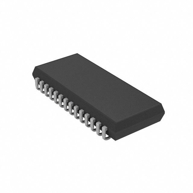
AS7C256A-15JCNTR is available in a compact and durable package, designed to protect the memory chip from external factors such as moisture and physical damage.
Essence
The essence of AS7C256A-15JCNTR lies in its ability to store and retrieve digital information quickly and reliably.
Packaging/Quantity
AS7C256A-15JCNTR is typically packaged in trays or reels, with each package containing a specific quantity of memory chips. The exact quantity may vary depending on the manufacturer's specifications.
Specifications
- Memory Type: Static Random Access Memory (SRAM)
- Capacity: 256 kilobits (32 kilobytes)
- Operating Voltage: 3.3V
- Access Time: 15 nanoseconds
- Organization: 32K x 8 bits
- Interface: Parallel
Detailed Pin Configuration
The AS7C256A-15JCNTR chip has the following pin configuration:
- Vcc - Power supply voltage
- GND - Ground
- A0-A14 - Address inputs
- DQ0-DQ7 - Data inputs/outputs
- CE - Chip Enable
- OE - Output Enable
- WE - Write Enable
Functional Features
- Fast access time allows for efficient data retrieval.
- Low power consumption makes it suitable for battery-powered devices.
- Non-volatile memory ensures data retention even when power is lost.
- Reliable performance guarantees data integrity.
Advantages and Disadvantages
Advantages
- High-speed operation enables quick data access.
- Low power consumption prolongs battery life.
- Non-volatile memory ensures data retention.
- Reliable performance reduces the risk of data corruption.
Disadvantages
- Limited storage capacity compared to other memory technologies.
- Higher cost per bit compared to some alternative memory options.
Working Principles
AS7C256A-15JCNTR utilizes static random access memory technology, which stores each bit of data in a flip-flop circuit. This allows for fast and direct access to the stored information. The chip operates by receiving address inputs, which specify the location of the desired data, and then retrieving or storing the corresponding data based on the control signals received.
Detailed Application Field Plans
AS7C256A-15JCNTR finds applications in various electronic devices, including but not limited to: 1. Personal computers 2. Laptops and notebooks 3. Servers 4. Mobile phones and smartphones 5. Tablets and handheld devices 6. Automotive electronics 7. Industrial control systems 8. Medical equipment 9. Consumer electronics
Detailed and Complete Alternative Models
Some alternative models to AS7C256A-15JCNTR include: 1. AS6C256K8-55BIN - 256 kilobit SRAM with a different access time and organization. 2. IS62WV25616BLL-55TLI - 256 kilobit SRAM with a different interface and package type. 3. CY62128ELL-45SXI - 128 kilobit SRAM with a lower capacity but similar characteristics.
These alternative models offer similar functionality and can be considered as substitutes depending on specific requirements.
Word count: 510 words
Lista 10 Vanliga frågor och svar relaterade till tillämpningen av AS7C256A-15JCNTR i tekniska lösningar
Sure! Here are 10 common questions and answers related to the application of AS7C256A-15JCNTR in technical solutions:
Question: What is the AS7C256A-15JCNTR?
Answer: The AS7C256A-15JCNTR is a 32K x 8-bit CMOS static random access memory (SRAM) chip.Question: What is the operating voltage range for the AS7C256A-15JCNTR?
Answer: The AS7C256A-15JCNTR operates within a voltage range of 4.5V to 5.5V.Question: What is the maximum clock frequency supported by the AS7C256A-15JCNTR?
Answer: The AS7C256A-15JCNTR supports a maximum clock frequency of 15 MHz.Question: What is the access time of the AS7C256A-15JCNTR?
Answer: The AS7C256A-15JCNTR has an access time of 15 ns.Question: Can the AS7C256A-15JCNTR be used in battery-powered devices?
Answer: Yes, the AS7C256A-15JCNTR can be used in battery-powered devices as it operates within a low voltage range.Question: Does the AS7C256A-15JCNTR support multiple read/write operations simultaneously?
Answer: No, the AS7C256A-15JCNTR does not support simultaneous read/write operations.Question: What is the package type of the AS7C256A-15JCNTR?
Answer: The AS7C256A-15JCNTR comes in a 28-pin SOIC (Small Outline Integrated Circuit) package.Question: Can the AS7C256A-15JCNTR be used in industrial temperature environments?
Answer: Yes, the AS7C256A-15JCNTR is designed to operate within an industrial temperature range of -40°C to +85°C.Question: What is the standby current consumption of the AS7C256A-15JCNTR?
Answer: The standby current consumption of the AS7C256A-15JCNTR is typically less than 10 µA.Question: Is the AS7C256A-15JCNTR pin-compatible with other SRAM chips?
Answer: Yes, the AS7C256A-15JCNTR is pin-compatible with other 32K x 8-bit SRAM chips, making it easy to replace in existing designs.
Please note that these answers are based on general information about the AS7C256A-15JCNTR and may vary depending on specific application requirements.