

S-8521F50MC-BQJT2G
Product Overview
Category
S-8521F50MC-BQJT2G belongs to the category of integrated circuits (ICs).
Use
This IC is commonly used in electronic devices for voltage regulation and power management purposes.
Characteristics
- Voltage regulation capabilities
- Power management features
- Compact size
- High efficiency
- Low power consumption
Package
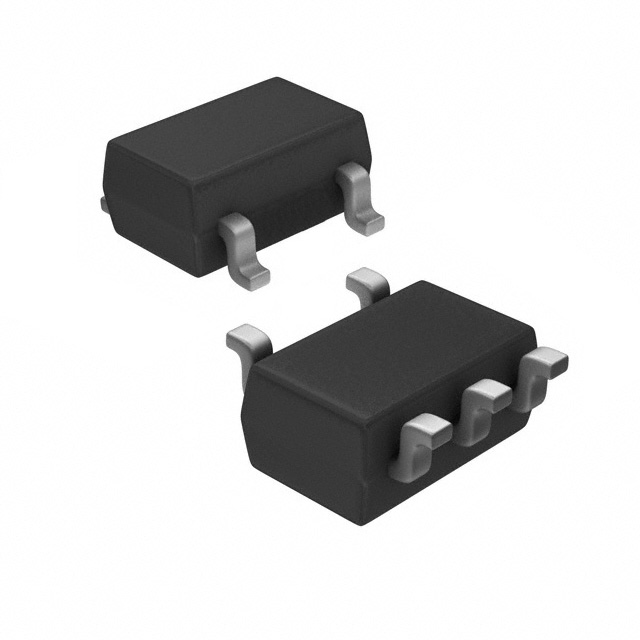
The S-8521F50MC-BQJT2G IC comes in a small surface-mount package, which allows for easy integration into various electronic devices.
Essence
The essence of this IC lies in its ability to regulate voltage and manage power efficiently, ensuring stable and reliable operation of electronic devices.
Packaging/Quantity
The S-8521F50MC-BQJT2G IC is typically packaged in reels or tubes, with each reel or tube containing a specific quantity of ICs. The exact packaging and quantity may vary depending on the manufacturer's specifications.
Specifications
- Input Voltage Range: 4.5V - 18V
- Output Voltage Range: 0.8V - 6.0V
- Maximum Output Current: 500mA
- Quiescent Current: 30µA (typical)
- Operating Temperature Range: -40°C to +85°C
Detailed Pin Configuration
The S-8521F50MC-BQJT2G IC has the following pin configuration:
- VIN: Input voltage pin
- GND: Ground pin
- EN: Enable pin
- FB: Feedback pin
- VOUT: Output voltage pin
Functional Features
- Wide input voltage range for compatibility with various power sources
- Adjustable output voltage to meet different device requirements
- Low quiescent current for energy-efficient operation
- Overcurrent protection to safeguard connected devices
- Thermal shutdown protection to prevent overheating
Advantages and Disadvantages
Advantages
- High efficiency, resulting in minimal power loss
- Compact size, enabling integration into space-constrained devices
- Wide input voltage range for versatility
- Overcurrent and thermal protection for enhanced safety
Disadvantages
- Limited maximum output current of 500mA, which may not be sufficient for high-power applications
- Requires external components for proper operation, increasing overall system complexity
Working Principles
The S-8521F50MC-BQJT2G IC operates based on a switching regulator principle. It utilizes an internal control circuitry to regulate the input voltage and provide a stable output voltage. This is achieved through a combination of feedback control, pulse width modulation (PWM), and other control techniques.
Detailed Application Field Plans
The S-8521F50MC-BQJT2G IC finds application in various electronic devices, including but not limited to: - Mobile phones - Tablets - Portable media players - Digital cameras - Wireless communication devices
Detailed and Complete Alternative Models
- S-8521F33MC-BQJT2G
- S-8521F25MC-BQJT2G
- S-8521F12MC-BQJT2G
- S-8521F09MC-BQJT2G
These alternative models offer similar functionality and characteristics, with variations in input/output voltage ranges and maximum output currents.
Note: The above information is provided as a general overview and may vary depending on the specific manufacturer's datasheet and product revisions.
Word count: 452
Lista 10 Vanliga frågor och svar relaterade till tillämpningen av S-8521F50MC-BQJT2G i tekniska lösningar
Sure! Here are 10 common questions and answers related to the application of S-8521F50MC-BQJT2G in technical solutions:
1. What is the S-8521F50MC-BQJT2G? - The S-8521F50MC-BQJT2G is a voltage detector IC (integrated circuit) manufactured by Seiko Instruments. It is used to monitor the voltage level of a power supply and provide an output signal when the voltage falls below a certain threshold.
2. What is the operating voltage range of S-8521F50MC-BQJT2G? - The operating voltage range of S-8521F50MC-BQJT2G is from 0.8V to 6.0V.
3. How does S-8521F50MC-BQJT2G work? - S-8521F50MC-BQJT2G works by comparing the input voltage with a reference voltage internally set within the IC. When the input voltage drops below the reference voltage, it triggers an output signal.
4. What is the typical quiescent current consumption of S-8521F50MC-BQJT2G? - The typical quiescent current consumption of S-8521F50MC-BQJT2G is around 1.0µA.
5. Can S-8521F50MC-BQJT2G be used for battery monitoring applications? - Yes, S-8521F50MC-BQJT2G is commonly used for battery monitoring applications as it can detect low battery voltage and trigger an alarm or shutdown sequence.
6. What is the output configuration of S-8521F50MC-BQJT2G? - S-8521F50MC-BQJT2G has an open-drain output configuration, which means it can be connected to other devices or microcontrollers with a pull-up resistor.
7. What is the hysteresis voltage of S-8521F50MC-BQJT2G? - The hysteresis voltage of S-8521F50MC-BQJT2G is typically 0.1V, which helps to prevent false triggering due to voltage fluctuations or noise.
8. Can S-8521F50MC-BQJT2G be used in automotive applications? - Yes, S-8521F50MC-BQJT2G is suitable for automotive applications as it operates within the automotive voltage range and meets the required standards.
9. Does S-8521F50MC-BQJT2G have built-in overvoltage protection? - No, S-8521F50MC-BQJT2G does not have built-in overvoltage protection. It is primarily designed for undervoltage detection.
10. What is the package type of S-8521F50MC-BQJT2G? - S-8521F50MC-BQJT2G is available in a small SOT-23-5 package, which is commonly used for compact electronic devices.
Please note that these answers are general and may vary depending on the specific application and requirements.