

S-80957CLNB-G7TT2G
Product Overview
Category
S-80957CLNB-G7TT2G belongs to the category of integrated circuits (ICs).
Use
This IC is commonly used in electronic devices for voltage detection and reset functions.
Characteristics
- Voltage detection range: 1.6V to 6.0V
- Low supply current: 1.0μA (typical)
- High accuracy voltage detection: ±1.0%
- Built-in delay circuit: 50ms (typical)
- Small package size: SOT-23-5
- RoHS compliant
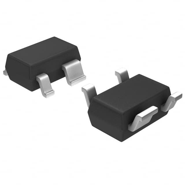
Package
The S-80957CLNB-G7TT2G IC is packaged in a compact SOT-23-5 package, which consists of five pins.
Essence
The essence of this product lies in its ability to accurately detect voltage levels within a specified range and provide a reset signal when necessary.
Packaging/Quantity
The S-80957CLNB-G7TT2G IC is typically available in reels containing 3,000 units per reel.
Specifications
- Supply voltage range: 1.6V to 6.0V
- Operating temperature range: -40°C to +85°C
- Output type: Active low
- Quiescent current: 1.0μA (typical)
- Accuracy: ±1.0%
- Delay time: 50ms (typical)
- Power dissipation: 200mW (max)
Detailed Pin Configuration
The S-80957CLNB-G7TT2G IC has the following pin configuration:
```
| | --| VDD|-- Pin 1: Supply Voltage --| GND|-- Pin 2: Ground --| RST|-- Pin 3: Reset Output --| VIN|-- Pin 4: Voltage Input |____| ```
Functional Features
- Voltage Detection: The IC accurately detects the input voltage within the specified range.
- Reset Function: When the voltage falls below the detection threshold, the IC generates a reset signal.
- Delay Circuit: The built-in delay circuit ensures a stable reset signal by introducing a delay of 50ms.
Advantages and Disadvantages
Advantages
- Wide voltage detection range allows for versatile applications.
- High accuracy ensures reliable voltage detection.
- Low supply current minimizes power consumption.
- Small package size enables space-saving designs.
- RoHS compliance promotes environmental friendliness.
Disadvantages
- Limited to voltage detection and reset functions, may not suit all application requirements.
- Requires external components for complete functionality.
Working Principles
The S-80957CLNB-G7TT2G IC operates based on a voltage divider network connected to the VIN pin. It compares the divided voltage with an internal reference voltage to determine if it falls within the specified range. If the voltage drops below the detection threshold, the IC triggers the reset output pin (RST) to generate a reset signal.
Detailed Application Field Plans
The S-80957CLNB-G7TT2G IC finds applications in various electronic devices that require voltage monitoring and reset capabilities. Some potential application fields include:
- Microcontrollers: Ensuring proper system initialization and preventing data corruption during power fluctuations.
- Battery-Powered Devices: Monitoring battery voltage levels and triggering low-battery warnings or shutdowns.
- Power Management Systems: Providing voltage supervision and reset functions for efficient power control.
- Industrial Automation: Enabling fault detection and system recovery in critical control circuits.
Detailed and Complete Alternative Models
- S-80930CNMC-G8XT2G: Similar voltage detection and reset IC with a different package (SOT-23-5).
- S-80942CNMC-G8XT2G: Voltage detection and reset IC with a wider voltage range and adjustable delay time.
- S-80960CNMC-G8XT2G: High-accuracy voltage detection and reset IC with an extended temperature range.
These alternative models offer similar functionalities to the S-80957CLNB-G7TT2G IC, catering to different application requirements.
Word count: 604 words
Lista 10 Vanliga frågor och svar relaterade till tillämpningen av S-80957CLNB-G7TT2G i tekniska lösningar
Sure! Here are 10 common questions and answers related to the application of S-80957CLNB-G7TT2G in technical solutions:
Q: What is the operating voltage range of S-80957CLNB-G7TT2G? A: The operating voltage range is from 1.6V to 6.0V.
Q: What is the typical quiescent current consumption of this device? A: The typical quiescent current consumption is 1.0µA.
Q: Can S-80957CLNB-G7TT2G be used as a voltage supervisor for microcontrollers? A: Yes, it can be used as a voltage supervisor for microcontrollers and other digital ICs.
Q: Does this device have an adjustable reset threshold voltage? A: No, the reset threshold voltage is fixed at 2.93V.
Q: Is S-80957CLNB-G7TT2G suitable for battery-powered applications? A: Yes, it is suitable for battery-powered applications due to its low quiescent current.
Q: What is the maximum supply voltage that this device can handle? A: The maximum supply voltage is 6.0V.
Q: Can S-80957CLNB-G7TT2G provide a manual reset input? A: No, this device does not have a manual reset input.
Q: Does this device have built-in hysteresis for the reset output? A: Yes, it has a built-in hysteresis of typically 100mV.
Q: Can S-80957CLNB-G7TT2G be used in automotive applications? A: Yes, it is suitable for automotive applications as it meets AEC-Q100 standards.
Q: What is the package type of S-80957CLNB-G7TT2G? A: It is available in a SOT-23-5 package.
Please note that these answers are based on general information and may vary depending on the specific application requirements.