

S-80933CLNB-G63T2G
Product Overview
Category
S-80933CLNB-G63T2G belongs to the category of integrated circuits (ICs).
Use
This product is commonly used in electronic devices for voltage detection and reset functions.
Characteristics
- Voltage detection range: 1.6V to 6.0V
- Accuracy: ±1.0%
- Low supply current: 1.0μA (typ.)
- Reset output type: N-channel open drain
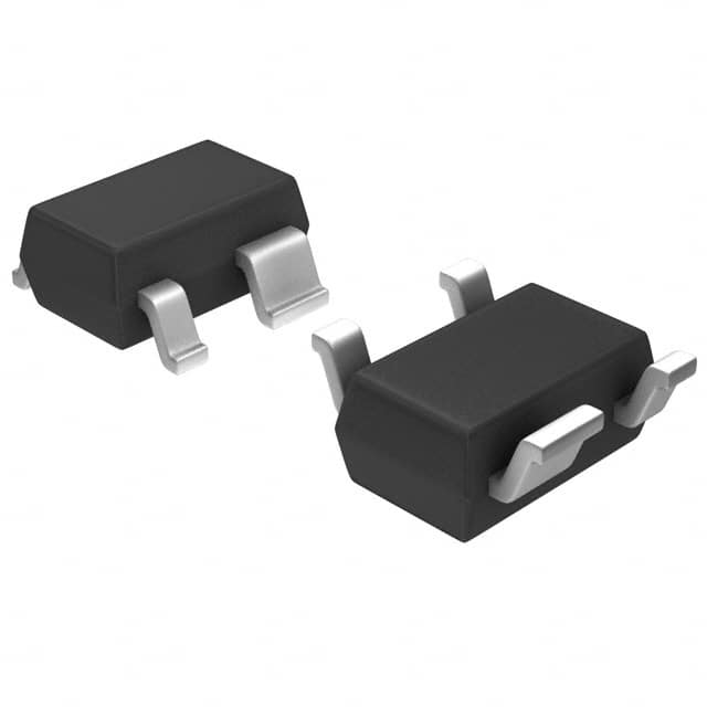
- Package type: SOT-23-5
- Operating temperature range: -40°C to +85°C
Package and Quantity
The S-80933CLNB-G63T2G is available in a SOT-23-5 package. Each package contains one unit of the IC.
Specifications
Pin Configuration
The S-80933CLNB-G63T2G has the following pin configuration:
| Pin Number | Pin Name | Description | |------------|----------|-------------| | 1 | VDD | Power supply input | | 2 | GND | Ground | | 3 | RESET | Reset output | | 4 | MR | Manual reset input | | 5 | VOUT | Output voltage |
Functional Features
- Voltage detection: The S-80933CLNB-G63T2G can accurately detect voltages within the range of 1.6V to 6.0V.
- Reset function: It provides a reset output signal when the detected voltage falls below a specified threshold.
- Manual reset: The MR pin allows for manual resetting of the device.
- Low power consumption: With a supply current of only 1.0μA, this IC minimizes power consumption in electronic devices.
Advantages
- Wide voltage detection range allows for versatile applications.
- Accurate voltage detection with low tolerance ensures reliable operation.
- Low power consumption prolongs battery life in portable devices.
- Compact SOT-23-5 package enables space-saving integration.
Disadvantages
- Limited to voltage detection and reset functions, may not be suitable for complex applications requiring additional features.
- The open-drain reset output requires an external pull-up resistor for proper signal level translation.
Working Principles
The S-80933CLNB-G63T2G operates based on a voltage divider network connected to the VDD pin. When the detected voltage falls below the threshold, the reset output is activated, indicating a low-voltage condition. The MR pin can be used to manually reset the device.
Application Field Plans
The S-80933CLNB-G63T2G finds applications in various electronic devices where voltage monitoring and reset functionality are required. Some potential application fields include: 1. Battery-powered devices: Ensuring safe operation by monitoring battery voltage and triggering a reset when it drops below a critical level. 2. Microcontroller systems: Providing a reliable reset signal to the microcontroller during power-up or voltage fluctuations. 3. Industrial equipment: Monitoring power supply voltages to prevent damage or malfunctioning of sensitive components.
Alternative Models
For those seeking alternative options, the following models offer similar functionality: 1. S-80934CLNB-G63T2G 2. S-80935CLNB-G63T2G 3. S-80936CLNB-G63T2G
These models have comparable specifications and pin configurations, making them suitable alternatives to the S-80933CLNB-G63T2G.
In conclusion, the S-80933CLNB-G63T2G is an integrated circuit designed for voltage detection and reset functions. With its wide voltage detection range, accuracy, and low power consumption, it offers reliable performance in various electronic devices. Its compact package and availability of alternative models make it a versatile choice for designers in need of voltage monitoring solutions.
Word count: 452
Lista 10 Vanliga frågor och svar relaterade till tillämpningen av S-80933CLNB-G63T2G i tekniska lösningar
What is the operating voltage range of S-80933CLNB-G63T2G?
- The operating voltage range of S-80933CLNB-G63T2G is 0.7V to 6.0V.What is the typical quiescent current of S-80933CLNB-G63T2G?
- The typical quiescent current of S-80933CLNB-G63T2G is 1.0μA.Can S-80933CLNB-G63T2G be used in battery-powered applications?
- Yes, S-80933CLNB-G63T2G is suitable for battery-powered applications due to its low quiescent current.What is the output voltage accuracy of S-80933CLNB-G63T2G?
- The output voltage accuracy of S-80933CLNB-G63T2G is ±2.0%.Is S-80933CLNB-G63T2G suitable for use in automotive electronics?
- Yes, S-80933CLNB-G63T2G is AEC-Q100 qualified and can be used in automotive electronics.What is the maximum output current of S-80933CLNB-G63T2G?
- The maximum output current of S-80933CLNB-G63T2G is 0.1A.Can S-80933CLNB-G63T2G withstand reverse polarity?
- No, S-80933CLNB-G63T2G cannot withstand reverse polarity. Proper circuit protection should be implemented.What is the temperature range for S-80933CLNB-G63T2G?
- The temperature range for S-80933CLNB-G63T2G is -40°C to 125°C.Does S-80933CLNB-G63T2G have built-in overcurrent protection?
- Yes, S-80933CLNB-G63T2G has built-in overcurrent protection.Is S-80933CLNB-G63T2G available in a small package size?
- Yes, S-80933CLNB-G63T2G is available in a compact SOT-23-5 package.