

S-80932CLPF-G62TFU
Product Overview
Category
S-80932CLPF-G62TFU belongs to the category of integrated circuits (ICs).
Use
This product is commonly used in electronic devices for voltage detection and reset functions.
Characteristics
- Voltage detection range: 2.0V to 6.0V
- Low supply current: 1.0µA (typ.)
- Reset output type: N-channel open drain
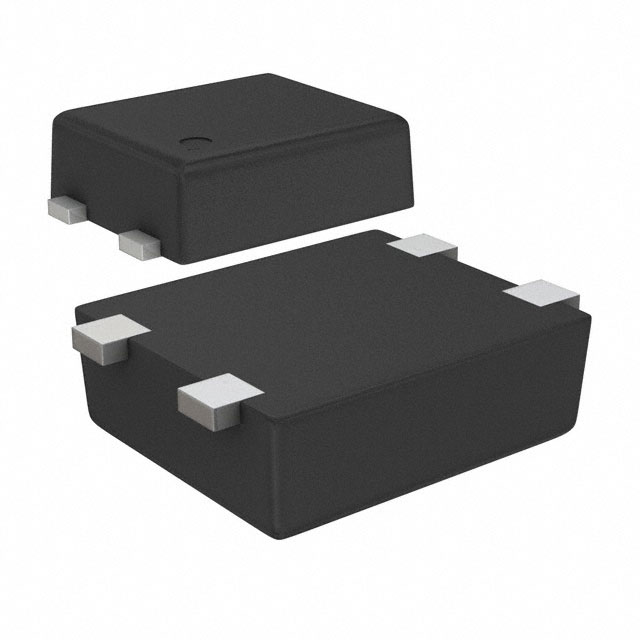
- Package type: SOT-23-5
- Operating temperature range: -40°C to +85°C
Package and Quantity
The S-80932CLPF-G62TFU is available in a SOT-23-5 package. It is typically sold in reels containing 3,000 units.
Specifications
- Supply voltage range: 1.0V to 10.0V
- Detection voltage accuracy: ±1.0%
- Quiescent current: 1.0µA (typ.)
- Output leakage current: 1.0µA (max)
- Power-on reset time: 20ms (typ.)
Detailed Pin Configuration
The S-80932CLPF-G62TFU has five pins arranged as follows:
```
| | --| |-- |____| ```
Pin 1: VDD (Supply voltage) Pin 2: GND (Ground) Pin 3: RESET (Reset output) Pin 4: CE (Chip enable) Pin 5: MR (Manual reset)
Functional Features
- Voltage detection with high accuracy
- Low power consumption
- Open-drain reset output for easy integration with other components
- Manual reset function for system control
Advantages and Disadvantages
Advantages
- Wide operating voltage range
- Accurate voltage detection
- Low power consumption
- Compact package size for space-constrained applications
Disadvantages
- Limited reset output current capacity
- Manual reset function may require additional external components
Working Principles
The S-80932CLPF-G62TFU operates by monitoring the supply voltage and generating a reset signal when it falls below a certain threshold. The chip enable (CE) pin allows the device to be enabled or disabled, while the manual reset (MR) pin provides a means to manually trigger a system reset.
Detailed Application Field Plans
The S-80932CLPF-G62TFU is widely used in various electronic devices that require reliable voltage detection and reset functionality. Some common application fields include:
- Battery-powered devices: Ensures proper operation and prevents damage due to low battery voltage.
- Microcontrollers and microprocessors: Provides a reset signal during power-up or voltage fluctuations to ensure stable system operation.
- Industrial control systems: Monitors power supply voltages to prevent malfunctions and protect sensitive equipment.
- Automotive electronics: Detects abnormal voltage conditions and triggers appropriate actions to safeguard critical systems.
Detailed and Complete Alternative Models
- S-80930CLPF-G6ZTFG: Similar specifications and features, but with a different package (SOT-89-5).
- S-80933CNPF-G8XTFG: Higher voltage detection range (2.0V to 10.0V) and lower quiescent current (0.5µA typ.), but with a different pin configuration (SOT-23-5).
These alternative models offer similar functionality and can be considered as substitutes for the S-80932CLPF-G62TFU in various applications.
Word count: 470 words
Lista 10 Vanliga frågor och svar relaterade till tillämpningen av S-80932CLPF-G62TFU i tekniska lösningar
Sure! Here are 10 common questions and answers related to the application of S-80932CLPF-G62TFU in technical solutions:
Q: What is the purpose of S-80932CLPF-G62TFU? A: S-80932CLPF-G62TFU is a voltage detector IC designed for use in various technical solutions.
Q: What is the operating voltage range of S-80932CLPF-G62TFU? A: The operating voltage range of S-80932CLPF-G62TFU is typically between 1.6V and 6.0V.
Q: How does S-80932CLPF-G62TFU detect voltage levels? A: S-80932CLPF-G62TFU uses a built-in voltage reference and comparator to detect voltage levels.
Q: Can S-80932CLPF-G62TFU be used in battery-powered applications? A: Yes, S-80932CLPF-G62TFU can be used in battery-powered applications due to its low power consumption.
Q: What is the output configuration of S-80932CLPF-G62TFU? A: S-80932CLPF-G62TFU has an open-drain output configuration.
Q: What is the typical quiescent current of S-80932CLPF-G62TFU? A: The typical quiescent current of S-80932CLPF-G62TFU is very low, usually around 1.0µA.
Q: Is S-80932CLPF-G62TFU suitable for overvoltage protection? A: No, S-80932CLPF-G62TFU is not specifically designed for overvoltage protection.
Q: Can S-80932CLPF-G62TFU be used in automotive applications? A: Yes, S-80932CLPF-G62TFU is suitable for automotive applications as it meets the necessary standards.
Q: What is the temperature range of operation for S-80932CLPF-G62TFU? A: The temperature range of operation for S-80932CLPF-G62TFU is typically between -40°C and +85°C.
Q: Does S-80932CLPF-G62TFU have any built-in delay circuitry? A: No, S-80932CLPF-G62TFU does not have any built-in delay circuitry.