

AAT2848IDG-T1
Product Overview
Category
AAT2848IDG-T1 belongs to the category of integrated circuits (ICs).
Use
This product is commonly used in electronic devices for power management applications.
Characteristics
- Integrated circuit
- Power management functionality
- Small form factor
- High efficiency
- Low power consumption
Package
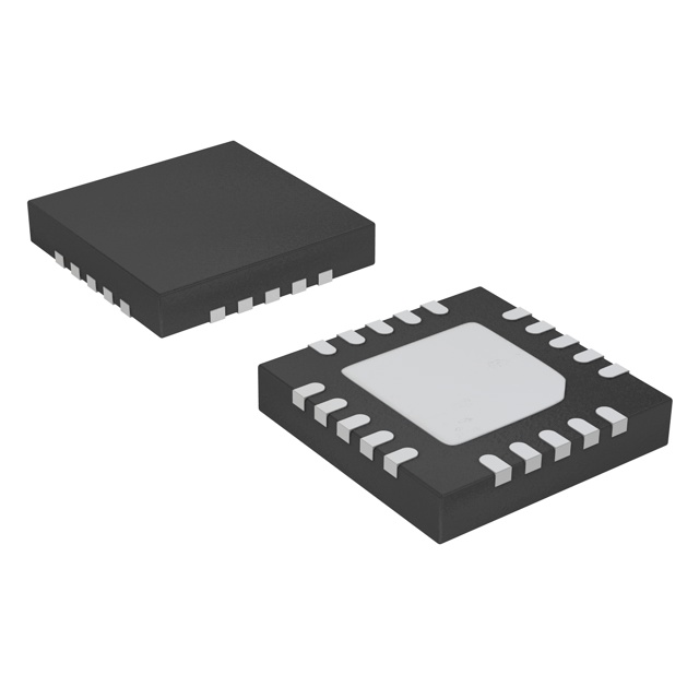
AAT2848IDG-T1 is available in a compact and industry-standard package, such as a 16-pin QFN (Quad Flat No-Lead) package.
Essence
The essence of AAT2848IDG-T1 lies in its ability to efficiently manage power in electronic devices, ensuring optimal performance and energy conservation.
Packaging/Quantity
This product is typically packaged in reels or tubes, with a quantity of 2500 units per reel/tube.
Specifications
- Input Voltage Range: 2.7V to 5.5V
- Output Voltage Range: Adjustable from 0.6V to VIN
- Maximum Output Current: 3A
- Switching Frequency: Up to 2MHz
- Operating Temperature Range: -40°C to +85°C
Detailed Pin Configuration
The AAT2848IDG-T1 IC has a total of 16 pins, each serving a specific function. The pin configuration is as follows:
- VIN: Input voltage pin
- EN: Enable pin
- FB: Feedback pin
- AGND: Analog ground pin
- SW: Switch pin
- PGND: Power ground pin
- VOUT: Output voltage pin
- COMP: Compensation pin
- SS: Soft-start pin
- BST: Boost pin
- PG: Power good pin
- NC: No connection
- NC: No connection
- NC: No connection
- NC: No connection
- NC: No connection
Functional Features
- High-efficiency step-down converter
- Adjustable output voltage
- Overcurrent protection
- Thermal shutdown protection
- Soft-start function for controlled startup
- Power good indicator
Advantages and Disadvantages
Advantages
- High efficiency leads to reduced power consumption
- Compact form factor enables integration into space-constrained designs
- Wide input voltage range allows compatibility with various power sources
- Adjustable output voltage provides flexibility in different applications
- Comprehensive protection features enhance reliability and safety
Disadvantages
- Limited maximum output current may not be suitable for high-power applications
- Higher cost compared to non-integrated power management solutions
Working Principles
The AAT2848IDG-T1 operates as a step-down (buck) converter, converting a higher input voltage to a lower output voltage. It utilizes pulse-width modulation (PWM) techniques to regulate the output voltage based on the feedback received from the FB pin. The integrated circuit incorporates various control mechanisms to ensure stable and efficient power delivery.
Detailed Application Field Plans
The AAT2848IDG-T1 is widely used in various electronic devices that require efficient power management. Some of the common application fields include:
- Mobile devices: Smartphones, tablets, portable media players
- Wearable electronics: Smartwatches, fitness trackers
- IoT (Internet of Things) devices: Sensors, smart home devices
- Consumer electronics: Digital cameras, gaming consoles
- Industrial equipment: Automation systems, control panels
Detailed and Complete Alternative Models
- AAT2858IDG-T1: Similar to AAT2848IDG-T1 with enhanced output current capability (up to 5A).
- AAT2868IDG-T1: Step-up (boost) converter variant for applications requiring higher output voltage.
- AAT2838IDG-T1: Step-down converter with lower maximum output current (2A) but reduced cost.
These alternative models offer similar functionality to the AAT2848IDG-T1, catering to different power management requirements.
Word count: 536 words
Lista 10 Vanliga frågor och svar relaterade till tillämpningen av AAT2848IDG-T1 i tekniska lösningar
Sure! Here are 10 common questions and answers related to the application of AAT2848IDG-T1 in technical solutions:
Q1: What is the AAT2848IDG-T1? A1: The AAT2848IDG-T1 is a specific model of power management integrated circuit (PMIC) designed for use in various technical solutions.
Q2: What are the key features of the AAT2848IDG-T1? A2: Some key features of the AAT2848IDG-T1 include multiple voltage regulators, power sequencing, overcurrent protection, and thermal shutdown.
Q3: What technical solutions can benefit from using the AAT2848IDG-T1? A3: The AAT2848IDG-T1 can be used in a wide range of applications such as smartphones, tablets, portable devices, and other battery-powered systems.
Q4: How many voltage regulators does the AAT2848IDG-T1 have? A4: The AAT2848IDG-T1 has multiple voltage regulators, typically including a buck converter and LDOs (low-dropout regulators).
Q5: What is power sequencing, and why is it important? A5: Power sequencing refers to the order in which different power supplies are turned on or off. It is important to ensure proper functionality and prevent damage to components.
Q6: Does the AAT2848IDG-T1 provide overcurrent protection? A6: Yes, the AAT2848IDG-T1 includes overcurrent protection to safeguard against excessive current flow that could damage the circuitry.
Q7: What is thermal shutdown, and how does it work in the AAT2848IDG-T1? A7: Thermal shutdown is a safety feature that protects the IC from overheating. When the temperature exceeds a certain threshold, the AAT2848IDG-T1 will automatically shut down to prevent damage.
Q8: Can the AAT2848IDG-T1 be used in battery-powered systems? A8: Yes, the AAT2848IDG-T1 is suitable for battery-powered systems and can efficiently manage power consumption to extend battery life.
Q9: Are there any specific design considerations when using the AAT2848IDG-T1? A9: Some design considerations include proper heat dissipation, input/output voltage requirements, and component placement to ensure optimal performance.
Q10: Where can I find more information about the AAT2848IDG-T1? A10: You can refer to the datasheet provided by the manufacturer or visit their official website for detailed information on the AAT2848IDG-T1.